


S1C63000 CORE CPU MANUAL EPSON i
CONTENTS
S1C63000 CORE CPU MANUAL
PREFACE
This manual explains the architecture, operation and instruction of the core CPU S1C63 of the CMOS 4-bit
single chip microcomputer S1C63 Family.
Also, since the memory configuration and the peripheral circuit configuration is different for each device
of the S1C63 Family, you should refer to the respective manuals for specific details other than the basic
functions.
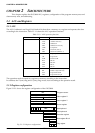
CONTENTS
CHAPTER 1OUTLINE ................................................................................................. 1
1.1 Features......................................................................................................... 1
1.2 Instruction Set Features ................................................................................ 1
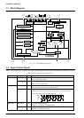
1.3 Block Diagram .............................................................................................. 2
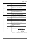
1.4 Input-Output Signals ..................................................................................... 2
CHAPTER 2ARCHITECTURE ........................................................................................ 4
2.1 ALU and Registers ........................................................................................ 4
2.1.1 ALU ............................................................................................................. 4
2.1.2 Register configuration ................................................................................ 4
2.1.3 Flags ........................................................................................................... 5
2.1.4 Arithmetic operations with numbering system............................................ 7
2.1.5 EXT register and data extension ................................................................. 8
2.2 Program Memory ......................................................................................... 11
2.2.1 Configuration of program memory ............................................................ 11
2.2.2 PC (program counter)................................................................................ 11
2.2.3 Branch instructions .................................................................................... 12
2.2.4 Table look-up instruction ........................................................................... 16
2.3 Data Memory ............................................................................................... 17
2.3.1 Configuration of data memory ................................................................... 17
2.3.2 Addressing for data memory ...................................................................... 18
2.3.3 Stack and stack pointer .............................................................................. 19
2.3.4 Memory mapped I/O .................................................................................. 21
CHAPTER 3 CPU OPERATION.................................................................................... 22
3.1 Timing Generator and Bus Cycle................................................................. 22
3.2 Instruction Fetch and Execution .................................................................. 22
3.3 Data Bus (Data Memory) Control ............................................................... 23
3.3.1 Data bus status........................................................................................... 23
3.3.2 High-impedance control ............................................................................ 23
3.3.3 Interrupt vector read .................................................................................. 24
3.3.4 Memory write ............................................................................................. 24
3.3.5 Memory read .............................................................................................. 25
3.4 Initial Reset .................................................................................................. 25
3.4.1 Initial reset sequence ................................................................................. 25
3.4.2 Initial setting of internal registers ............................................................. 26