


S1C63000 CORE CPU MANUAL EPSON 21
CHAPTER 2: ARCHITECTURE
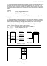
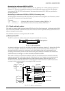
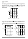
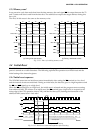
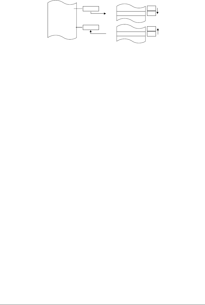
Fig. 2.3.3.4 4-bit stack operation
The SP2 increment/decrement affects only the 8-bit field shown in Figure 2.3.3.3, and its operation is
performed cyclically. In other words, if the SP2 is decremented by the PUSH instruction or other
conditions when the SP2 is 00H (indicating the memory address 0000H), the SP2 becomes FFH
(indicating the memory address 00FFH). Similarly, if the SP2 is incremented by the POP instruction or
other conditions when the SP2 is FFH (indicating the memory address 00FFH), the SP2 becomes 00H
(indicating the memory address 0000H).
(3) Notes for using the stack pointer
• The SP1 and SP2 are undefined at an initial reset. Therefore, both the stack pointers must be initialized
by software.
For safety, all the interrupts including NMI are masked until both the SP1 and SP2 are set by software.
Furthermore, if either the SP1 or SP2 is re-set, all the interrupts are masked again until the other is re-
set. Therefore be sure to set the SP1 and SP2 as a pair.
• The increment/decrement for the SP1 and SP2 is operated cyclically from 0000H to 03FFH (SP1) and
from 0000H to 00FFH (SP2) regardless of the memory capacity/allocation set up in each model.
Control with the program so that the stacks do not cross over the upper/lower limits of the mounted
memory.
• The SP1 must be set in the RAM area that permits 16-bit accessing depending on the model. The SP1
address stack cannot be allocated to other than the 16-bit accessible area even if the address is less
than 03FFH.
• The area management for the SP1 stack, SP2 stack and data RAM should be done by the user. Pay
attention to these areas so that they do not overlap in the same addresses.
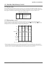
2.3.4 Memory mapped I/O
The S1C63 Family contains the S1C63000 as the core CPU and various types of peripheral circuits, such as
input/output ports. The S1C63000 has adopted a memory mapped I/O system for controlling the
peripheral circuits, and the control bits and the registers for exchanging data are arranged in the data
memory area.
The I/O memory for controlling the peripheral circuits is assigned to the area from FF00H to FFFFH, and
is distinguished from RAM and others. However, the accessing method is the same as RAM, so indirect
addressing can be done using the X or Y register. In addition, since the I/O memory is accessed fre-
quently, the exclusive instructions for this area are also provided. (See Section 2.3.2.)
Refer to the manual for the individual model of the S1C63 Family for the I/O memory and the peripheral
circuits.
PUSH A
Program memory
6H
:
:
A register
Stack (SP2)
50H
SP2
004FH
004EH
ROM
Address
6H
4FH
6H
A register
POP A
50H
SP2
004FH
004EH
6H
4FH