


68 MicroMAX System User Manual Version 6.C
On-Chip Binning
Binning is the process of adding the data from adjacent pixels together to form a single
pixel (som
etimes called a super-pixel), and it can be accomplished in either hardware or
software. Rectangular groups of pixels of any size may be binned together, subject to
some hardware and software limitations.
Hardware binning is performed before the signal is read out by
the preamplifier. For
signal levels that are readout noise limited this method improves S/N ratio linearly with
the number of pixels grouped together. For signals large enough to render the camera
photon shot noise limited, the S/N ratio improvement is roughly proportional to the
square-root of the number of pixels binned.
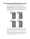
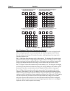
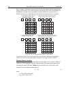
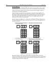
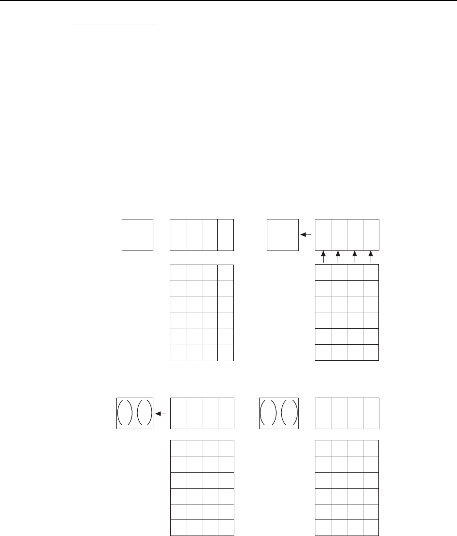
Figure 25 shows an example of 2 × 2 binning for a full fram
e CCD array. Each pixel of
the image displayed by the software represents 4 pixels of the array. Rectangular bins of
any size are possible
.
A2
A1
B2
B1
C2
C1
D2
D1
A4
A3
B4
B3
C4
C3
D4
D3
A6
A5
B6
B5
C6
C5
D6
D5
Empty Readout Register. Exposure has
ended and image is about to be shifted
into the Readout Register.
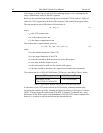
Charges from two lines in each column have
been shifted to Readout Register and added.
After sum of first four charges have been
transferred from Output Node, next four
charges are shifted into Output Node and added.
Four charges have been shifted to the
Output Node and added.
12
43
++++
+
+
+
++
C2 D2
C1 D1
+
+
+
A2 B2 C2 D2
A4
A3
B4
B3
C4
C3
D4
D3
A6
A5
B6
B5
C6
C5
D6
D5
A1 B1
C1 D1
A2 B2
A4
A3
B4
B3
C4
C3
D4
D3
A6
A5
B6
B5
C6
C5
D6
D5
A1 B1
C2 D2
A4
A3
B4
B3
C4
C3
D4
D3
A6
A5
B6
B5
C6
C5
D6
D5
C1 D1
Figure 25. 2 × 2 Binning for Full Frame CCD
Binning also reduces readout time and the burden on computer memory, but at the
expense of resolution. Since shift register pixels typically hold only twice as much charge
as image pixels, the binning of large sections may result in saturation and “blooming”, or
spilling of charge back into the image area.