


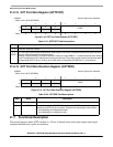
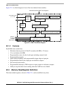
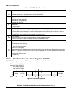
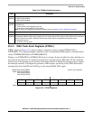

General Purpose Timer Module (GPT)
MCF52211 ColdFire® Integrated Microcontroller Reference Manual, Rev. 2
21-20 Freescale Semiconductor
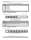
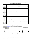
Table 21-23. GPT Settings and Pin Functions
GPTEN DDR
1
1
When DDR sets the pin as input (0), reading the data register returns the state of the pin. When DDR set the pin as output
(1), reading the data register returns the content of the data latch. Pin conditions such as rising or falling edges can trigger
an input capture on a pin configured as an input.
GPTIOS
EDGx
[B:A]
OMx/
OLx
2
2
OMn/OLn bit pairs select the output action to be taken as a result of a successful output compare. When OMn or OLn is set
and the IOSn bit is set, the pin is an output regardless of the state of the corresponding DDR bit.
OC3Mx
3
3
Setting an OC3M bit configures the corresponding PORTTn pin to be output. OC3Mn makes the PORTTn pin an output
regardless of the data direction bit when the pin is configured for output compare (IOSn = 1). The OC3Mn bits do not change
the state of the PORTTnDDR bits.
Pin
Data
Dir.
Pin
Driven
by
Pin
Function
Comments
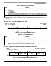
00X
4
4
X = Don’t care
X X X In Ext. Digital input GPT disabled by GPTEN = 0
0 1 X X X X Out Data reg. Digital output GPT disabled by GPTEN = 0
1 0 0 (IC) 0 (IC
disabled)
X 0 In Ext. Digital input Input capture disabled by EDGn
setting
1 1 0 0 X 0 Out Data reg. Digital output Input capture disabled by EDGn
setting
1 0 0 <> 0 X 0 In Ext. IC and
digital input
Normal settings for input capture
1 1 0 <> 0 X 0 Out Data reg. Digital output Input capture of data driven to output
pin by CPU
1 0 0 <> 0 X 1 In Ext. IC and
digital input
OC3M setting has no effect because
IOS = 0
1 1 0 <> 0 X 1 Out Data reg. Digital output OC3M setting has no effect because
IOS = 0; input capture of data driven
to output pin by CPU
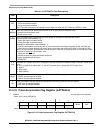
101 (OC)X
(3)
0
5
5
An output compare overrides the data direction bit of the output compare pin but does not change the state of the data
direction bit. Enabling output compare disables data register drive of the pin.
0 In Ext. Digital input Output compare takes place but
does not affect the pin because of
the OMn/OLn setting
1 1 1 X 0 0 Out Data reg. Digital output Output compare takes place but
does not affect the pin because of
the OMn/OLn setting
1 0 1 X <> 0 0 Out OC action Output
compare
Pin readable only if DDR = 0
(5)
1 1 1 X <> 0 0 Out OC action Output
compare
Pin driven by OC action
(5)
1 0 1 X X 1 Out OC action/
OC3Dn
Output
compare
(ch 3)
Pin readable only if DDR = 0
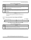
6
1 1 1 X X 1 Out OC action/
OC3Dn
Output
compare/
OC3Dn
(ch 3)
Pin driven by channel OC action and
OC3Dn via channel 3 OC
(6)