


ColdFire Core
MCF52211 ColdFire® Integrated Microcontroller Reference Manual, Rev. 2
3-4 Freescale Semiconductor
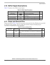
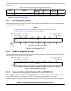
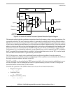
3.2.1 Data Registers (D0–D7)
D0–D7 data registers are for bit (1-bit), byte (8-bit), word (16-bit) and longword (32-bit) operations; they
can also be used as index registers.
NOTE
Registers D0 and D1 contain hardware configuration details after reset. See
Section 3.3.4.15, “Reset Exception” for more details.
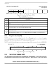
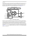
3.2.2 Address Registers (A0–A6)
These registers can be used as software stack pointers, index registers, or base address registers. They can
also be used for word and longword operations.
Figure 3-3. Address Registers (A0–A6)
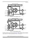
3.2.3 Supervisor/User Stack Pointers (A7 and OTHER_A7)
This ColdFire architecture supports two independent stack pointer (A7) registers—the supervisor stack
pointer (SSP) and the user stack pointer (USP). The hardware implementation of these two
program-visible 32-bit registers does not identify one as the SSP and the other as the USP. Instead, the
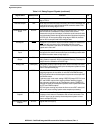
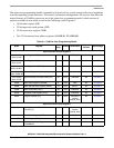
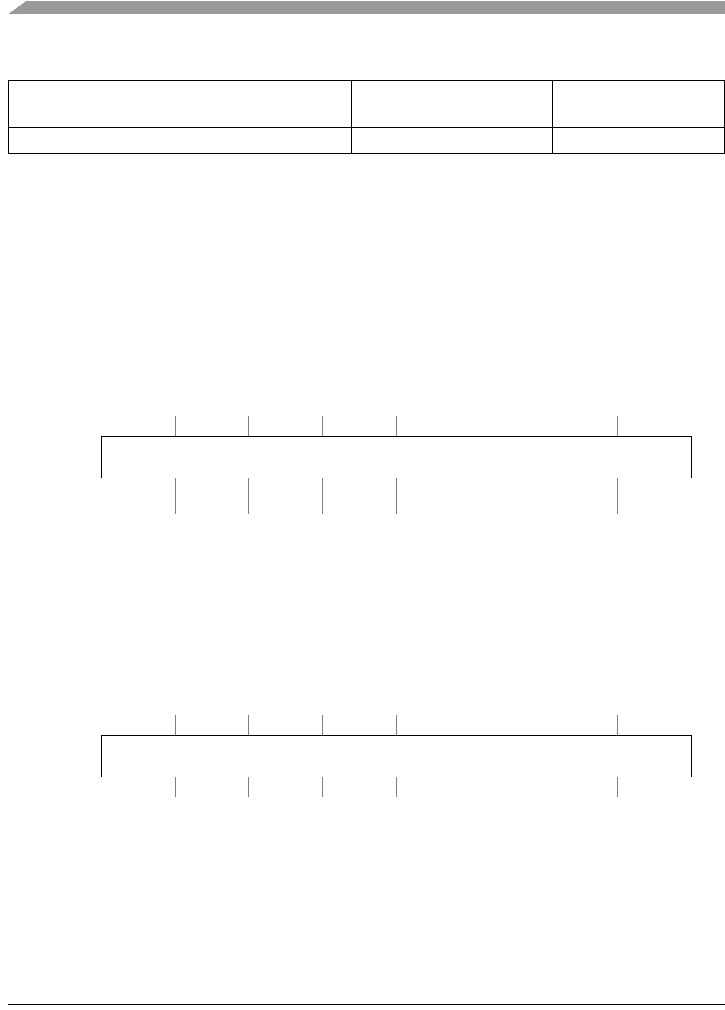
0xC05 RAM Base Address Register (RAMBAR) 32 R/W See Section Yes 3.2.8/3-8
1
The values listed in this column represent the Rc field used when accessing the core registers via the BDM port. For more
information see Chapter 28, “Debug Module”.
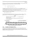
BDM: Load: 0x080 + n; n = 0-7 (Dn)
Store: 0x180 + n; n = 0-7 (Dn)
Access: User read/write
BDM read/write
313029282726252423222120191817161514131211109876543210
R
Data
W
Reset
(D2-D7)
––––––––––––––––––––––––––––––––
Reset
(D0, D1)
See Section 3.3.4.15, “Reset Exception”
Figure 3-2. Data Registers (D0–D7)
BDM: Load: 0x088 + n; n =0–6 (An)
Store: 0x188 + n; n =0–6 (An)
Access: User read/write
BDM read/write
313029282726252423222120191817161514131211109876543210
R
Address
W
Reset––––––––––––––––––––––––––––––––
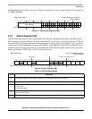
Table 3-1. ColdFire Core Programming Model (continued)
BDM
1
Register
Width
(bits)
Access Reset Value
Written with
MOVEC
Section/Page