


Debug Module
MCF52211 ColdFire® Integrated Microcontroller Reference Manual, Rev. 2
28-26 Freescale Semiconductor
• Results are returned in the two serial transfer cycles after the memory access completes. For any
command performing a byte-sized memory read operation, the upper 8 bits of the response data are
undefined and the referenced data is returned in the lower 8 bits. The next command’s opcode is
sent to the debug module during the final transfer. If a bus error terminates a memory or register
access, error status (S = 1, DATA = 0x0001) returns instead of result data.
28.5.3.3 Command Set Descriptions
The following sections describe the commands summarized in Table 28-20.
NOTE
The BDM status bit (S) is 0 for normally completed commands. S is set for
illegal commands, not-ready responses, and transfers with bus-errors.
Section 28.5.2, “BDM Serial Interface,” describes the receive packet
format.
Freescale reserves unassigned command opcodes for future expansion. Unused command formats in any
revision level perform a NOP and return an illegal command response.
28.5.3.3.1 Read A/D Register (RAREG/RDREG)
Read the selected address or data register and return the 32-bit result. A bus error response is returned if
the CPU core is not halted.
Command/Result Formats:
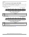
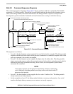
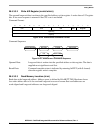
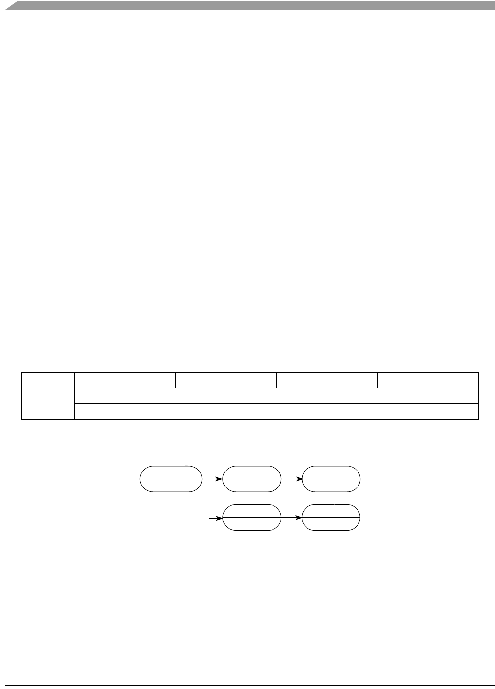
Command Sequence:
Figure 28-19. RAREG/RDREG Command Sequence
Operand Data: None
Result Data: The contents of the selected register are returned as a longword value,
most-significant word first.
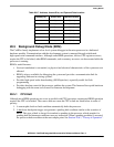
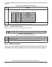
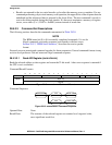
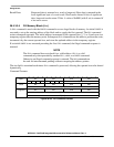
1514131211109876543210
Command 0x2 0x1 0x8 A/D Register
Result D[31:16]
D[15:0]
Figure 28-18. RAREG/RDREG Command Format
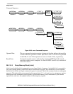
RAREG/RDREG
???
NEXT CMD
LS RESULT
NEXT CMD
’NOT READY’
XXX
BERR
XXX
MS RESULT