


Signal Descriptions
MCF52211 ColdFire® Integrated Microcontroller Reference Manual, Rev. 2
Freescale Semiconductor 2-11
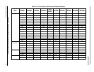
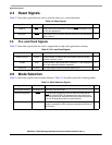
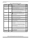
2.12 ADC Signals
Table 2-11 describes the signals of the analog-to-digital converter.
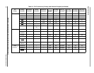
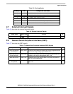
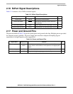
2.13 General Purpose Timer Signals
Table 2-12 describes the general purpose timer signals.
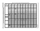
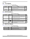
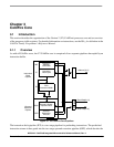
2.14 Pulse-Width Modulator Signals
Table 2-13 describes the PWM signals.
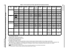
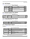
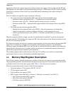
2.15 Debug Support Signals
The signals in Table 2-14 are used as the interface to the on-chip JTAG controller and also to interface to
the BDM logic.
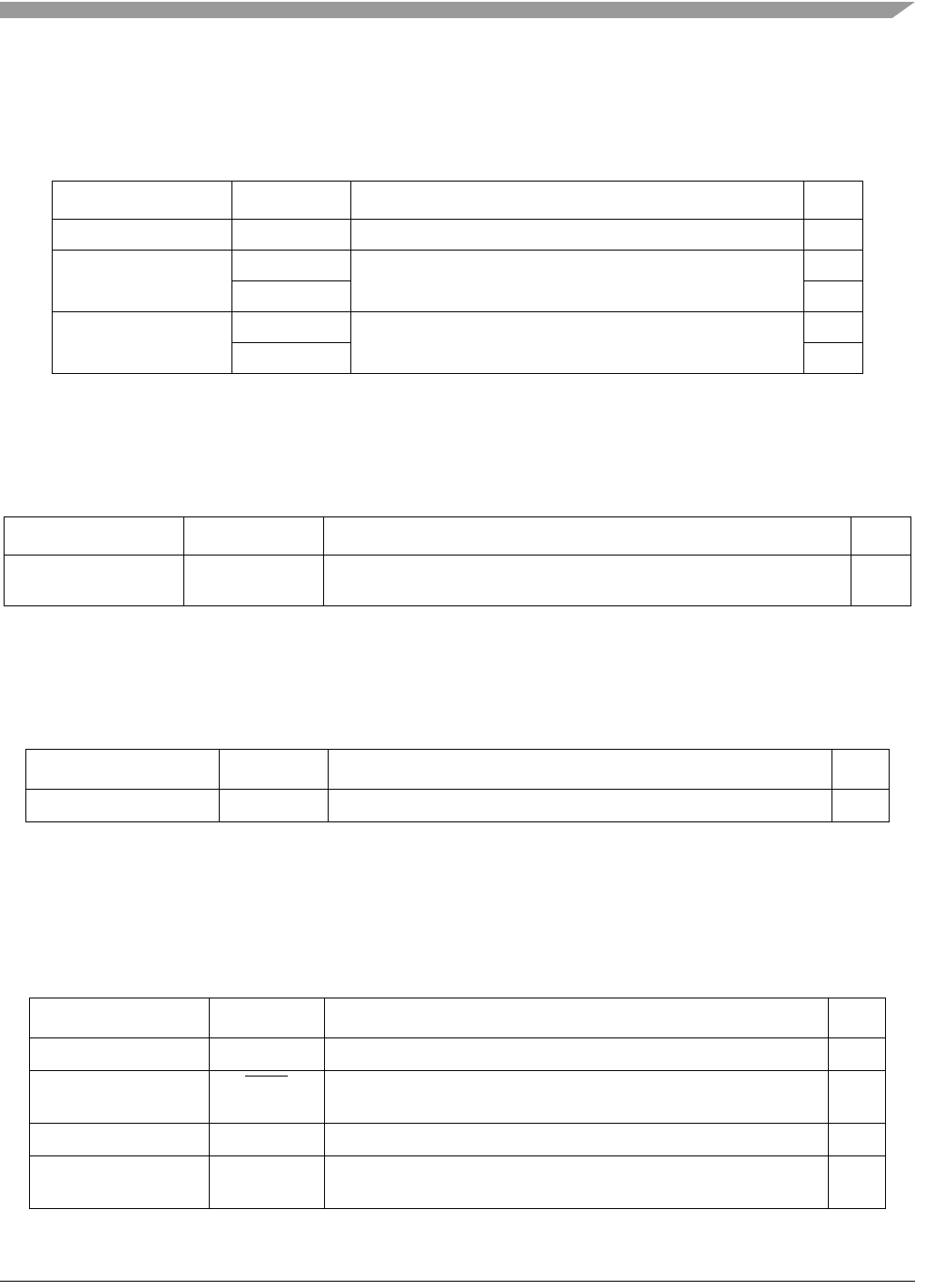
Table 2-11. ADC Signals
Signal Name Abbreviation Function I/O
Analog Inputs AN[7:0] Inputs to the ADC. I
Analog Reference V
RH
Reference voltage high and low inputs. I
V
RL
I
Analog Supply V
DDA
Isolate the ADC circuitry from power supply noise —
V
SSA
—
Table 2-12. GPT Signals
Signal Name Abbreviation Function I/O
General Purpose Timer
Input/Output
GPT[3:0] Inputs to or outputs from the general purpose timer module I/O
Table 2-13. PWM Signals
Signal Name Abbreviation Function I/O
PWM Output Channels PWM[7:0] Pulse-width modulated output for PWM channels O
Table 2-14. Debug Support Signals
Signal Name Abbreviation Function I/O
JTAG Enable JTAG_EN Select between debug module and JTAG signals at reset I
Test Reset TRST
This active-low signal is used to initialize the JTAG logic
asynchronously.
I
Test Clock TCLK Used to synchronize the JTAG logic. I
Test Mode Select TMS Used to sequence the JTAG state machine. TMS is sampled on the
rising edge of TCLK.
I