4
2
2
:
:
S
S
P
P
I
I
C
C
o
o
n
n
t
t
r
r
o
o
l
l
l
l
e
e
r
r
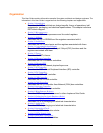
This chapter describes the DSTni Serial Peripheral Interface (SPI) controller. Topics include:
Theory of Operation on page 4
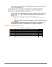
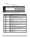
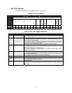
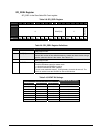
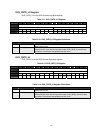
SPI Controller Register Summary on page 5
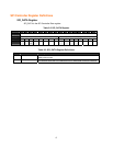
SPI Controller Register Definitions on page 6
Theory of Operation
SPI Background
SPI is a high-speed synchronous serial input/output (I/O) port that allows a serial bit stream of
programmed length (one to eight bits) to be shifted into and out of the device at a
programmable bit-transfer rate.
SPI is an industry-standard communications interface that does not have specifications or a
standards organizing group. As a result, there are no licensing requirements. Because of its
simplicity, SPI is commonly used in embedded systems. Many semiconductor manufacturers
sell a variety of sensor, conversion, and control devices that use SPI.
DSTni SPI Controller
The DSTni SPI controller is located at base I/O address B800h. It shares an interrupt with the
I
2
C controller and connects to interrupt 2. The SPI controller is enabled using the DSTni
Configuration register. If set to 1, the SPI controller is enabled on serial port 3. This bit can
reset to 1 with an external pull-up resistor. Normally it resets to 0 on reset or power-up.
The SPI bus is a 3-wire bus serial bus that links a serial shift register between a master device
and a slave device. This design supports both master and slave operations. Typically, master
and slave devices have an 8-bit shift register, for a combined register of 16 bits. During an SPI
transfer, the master and slave shift registers by eight bits and exchange their 8-bit register
values, starting with the most-significant bit.
The SPI interface is software configurable. The clock polarity, clock phase, SLVSEL polarity,
clock frequency in master mode, and number of bits to be transferred are all software
programmable. SPI supports multiple slaves on a single 3-wire bus by using separate Slave
Select signals to enable the desired slave. Multiple masters are also fully supported and some
support is provided for detecting collisions when multiple masters attempt to transfer at the
same time.
A Wired-OR mode is provided which allows multiple masters to collide on the bus without risk of
damage. In this mode, an external pull-up resistor is required on the Master Out Slave In
(MOSI) ) and Master In Slave Out (MISO) pins. The wired-OR mode also allows the SPI bus to
operate as a 2-wire bus by connecting the MOSI and MISO pins to form a single bi-directional
data pin. Generally, pull-ups are recommended on all of the external SPI signals to ensure they
are held in a valid state, even when the SPI interface is disabled. For some device connections,
the ALT mode bit will swap the TX and RX pins.
The SPI controller has an enhanced mode called AUTODRV. This mode is valid in master
mode. In this mode, the SLVSEL pin is driven active when data is written to the data register.
After the last bit of data is shifted out, the SLVSEL goes inactive and an interrupt is generated.
The INVCS bit can generate either a positive or negative true SLVSEL pin.


