28
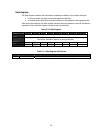
Clock Control Register
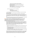
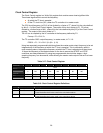
The Clock Control register is a Write Only register that contains seven least-significant bits.
These least-significant bits control the frequency:
At which the I
2
C bus is sampled.
Of the I
2
C clock line (SCL) when the I
2
C controller is in master mode.
The CPU clock frequency (of CLK) is first divided by a factor of 2
N
, where N is the value defined
by bits 2 – 0 of the Clock Control register. The output of this clock divider is F0. F0 is then
divided by a further factor of M+1, where M is the value defined by bits [6:3] of the Clock Control
register. The output of this clock divider is F1.
The I
2
C bus is sampled by the I
2
C controller at the frequency defined by F0.
Fsamp = F0 = CLK / 2
N
The I
2
C controller OSCL output frequency, in master mode, is F1 / 10:
FOSCL = F1 / 10 = CLK / (2
N
(M + 1) 10)
Using two separately programmable dividers allows the master mode output frequency to be set
independently of the frequency at which the I
2
C bus is sampled. This is particularly useful in
multi-master systems, because the frequency at which the I
2
C bus is sampled must be at least
10 times the frequency of the fastest master on the bus to ensure that START and STOP
conditions are always detected. By using two programmable clock divider stages, a high
sampling frequency can be ensured, while allowing the master mode output to be set to a lower
frequency.
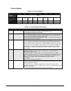
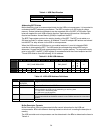
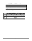
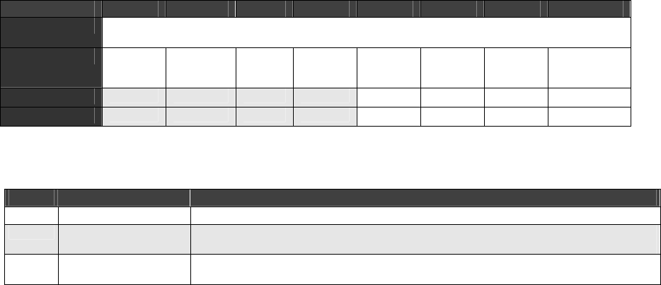
Table 3-17. Clock Control Register
BIT 7 6 5 4 3 2 1 0
OFFSET
D007
FIELD
/// M3 M2 M1 M0 N2 N1 N0
RESET
0 0 0 0 0 0 0 0
RW
W W W W W W W W
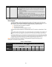
Table 3-18. Clock Control Register Definitions
Bits Field Name Description
7 ///
Reserved
6:3
M6 − M3
M Value
These bits define the M value used in the calculations above.
2:0
N2 − N0
N Value
These bits define the N value used in the calculations above


