


Ethernet AVB Endpoint User Guide www.xilinx.com 95
UG492 July 23, 2010
PLB Address Map and Register Definitions
This register and the registers defined in Table 10-6 and in Table 10-8 are linked. These
three offset values will be loaded into the RTC counter logic simultaneously following a
write to the nanosecond offset register defined in Table 10-6.
Table 10-8 describes the offset control register for the upper 16-bits of seconds field of the
“Real Time Clock,” used to force step changes into the counter. When in PTP clock master
mode, this can be used to set the initial value following power-up. When in PTP clock slave
mode, the “Software Drivers” use this register to implement the periodic step corrections.
This register and the registers defined in Table 10-6 and in Table 10-7 are linked. These
three offset values will be loaded into the RTC counter logic simultaneously following a
write to the nanosecond offset register defined in Table 10-6.
RTC Increment Value Control Register
Table 10-9 describes the RTC Increment Value Control Register. This provides
configurable increment rate for the “Real Time Clock” counter: this increment register
should simply take the value of the clock period which is being used to increment the RTC.
However, the resolution of this increment register is very fine (in units of 1/1048576
(1/2
20
) fraction of one nanosecond). Therefore, the RTC increment rate can be adjusted to
a very fine degree of accuracy. This provides the following features:
• The RTC can be incremented from any available clock frequency that is greater than
the P802.1AS defined minimum of 25 MHz.
• When acting as a clock slave, the rate adjustment of the RTC can be matched to that of
the network clock master to an exceptional level of accuracy.:
Current RTC Value Registers
Table 10-10 describes the nanoseconds field value register for the nanoseconds field of the
“Real Time Clock.” When read, this will return the latest value of the counter.
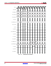
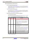
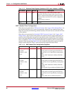
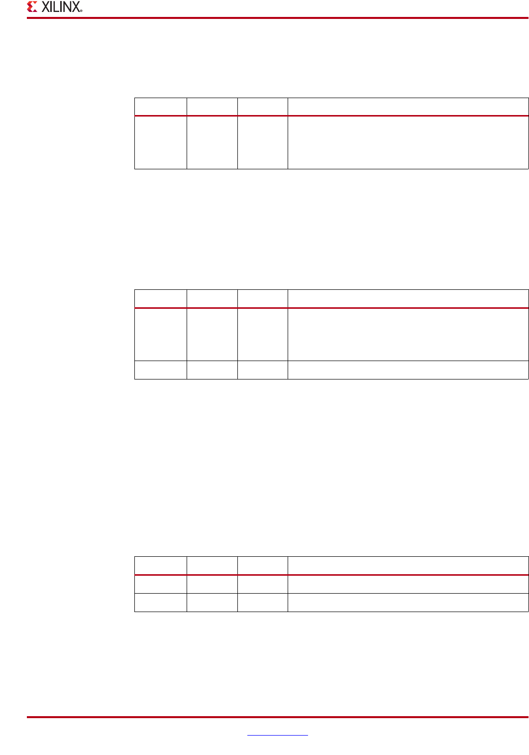
Table 10-7: Seconds Field Offset bits [31:0] (
PLB_base_address + 0x2808)
Bit no Default Access Description
31-0 0 R/W 32-bit offset value for the RTC seconds field (bits 31-0).
Used by the microprocessor to initialize the RTC, then
afterwards to perform the regular RTC corrections
(when in slave mode).
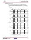
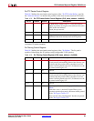
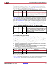
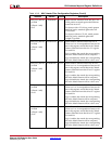
Table 10-8: Seconds Field Offset bits [47:32] (PLB_base_address + 0x280C)
Bit no Default Access Description
15-0 0 R/W 16-bit offset value for the RTC seconds field (bits 47-32).
Used by the microprocessor to initialize the RTC, then
afterwards to perform the regular RTC corrections
(when in slave mode).
31-16 0 RO Unused
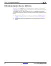
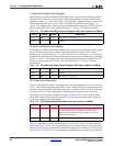
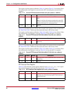
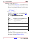
Table 10-9: RTC Increment Value Control Register (PLB_base_address + 0x2810)
Bit no Default Access Description
25-0 0 R/W Per rtc_clk clock period Increment Value for the RTC.
31-26 0 RO Unused