


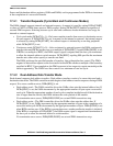

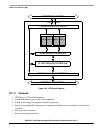

ColdFire Flash Module (CFM)
MCF52211 ColdFire® Integrated Microcontroller Reference Manual, Rev. 2
18-4 Freescale Semiconductor
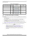
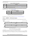
18.3.2 Flash Base Address Register (FLASHBAR)
The configuration information in the flash base address register (FLASHBAR) controls the operation of
the flash module.
• The FLASHBAR holds the base address of the flash. The MOVEC instruction provides write-only
access to this register.
• The FLASHBAR can be read or written from the debug module in a similar manner.
• All undefined bits in the register are reserved. These bits are ignored during writes to the
FLASHBAR and return zeroes when read from the debug module.
• The FLASHBAR valid bit is programmed according to the chip mode selected at reset (see
Chapter 9, “Chip Configuration Module (CCM)” for more details). All other bits are unaffected.
The FLASHBAR register contains several control fields. These fields are shown in Figure 18-3.
NOTE
The default value of the FLASHBAR is determined by the chip
configuration selected at reset (see Chapter 9, “Chip Configuration Module
(CCM)” for more information). If external boot mode is used, the
FLASHBAR located in the processor’s CPU space is invalid and it must be
initialized with the valid bit set before the CPU (or modules) can access the
on-chip flash.
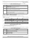
Table 18-1. CFM Configuration Field
Address Offset
(from PROGRAM_ARRAY_BASE)
Size
(bytes)
Description
Factory
Default
0x0400 - 0x0407 8 Backdoor Comparison Key 0xFFFF_FFFF_FFFF_FFF
F
0x0408 - 0x040B 4 Flash Protection Bytes
(see Section 18.3.3.4, “CFMPROT —
CFM Protection Register”)
0xFFFF_FFFF
0x040C - 0x040F 4 Flash SUPV Access Bytes
(see Section 18.3.3.5, “CFMSACC —
CFM Supervisor Access Register”)
0xFFFF_FFFF
0x0410 - 0x0413 4 Flash DATA Access Bytes
(see Section 18.3.3.6, “CFMDACC —
CFM Data Access Register”)
0xFFFF_FFFF
0x0414 - 0x0417 4 Flash Security Word
(see Section 18.3.3.3, “CFMSEC —
CFM Security Register”)
0xFFFF_FFFF