


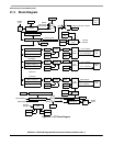

General Purpose Timer Module (GPT)
MCF52211 ColdFire® Integrated Microcontroller Reference Manual, Rev. 2
21-10 Freescale Semiconductor
21.6.9 GPT Control Register 2 (GPTCTL2)
21.6.10 GPT Interrupt Enable Register (GPTIE)
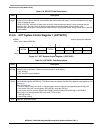
Table 21-11. GPTCL1 Field Descriptions
Field Description
7–0
OMx/OLx
Output mode/output level. Selects the output action to be taken as a result of a successful output compare on each
channel. When OMn or OLn is set and the IOSn bit is set, the pin is an output regardless of the state of the
corresponding DDR bit. These bits are read anytime, write anytime.
00 GPT disconnected from output pin logic
01 Toggle OCn output line
10 Clear OCn output line
11 Set OCn line
Note: Channel 3 shares a pin with the pulse accumulator input pin. To use the PAI input, clear the OM3 and OL3
bits and clear the OC3M3 bit in the output compare 3 mask register.
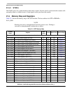
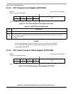
IPSBAR
Offset: 0x1A_000B (GPTCTL2)
Access: Supervisor read/write
76543210
R
EDG3B EDG3A EDG2B EDG2A EDG1B EDG1A EDG0B EDG0A
W
Reset:00000000
Figure 21-11. GPT Control Register 2(GPTCTL2)
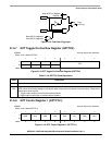
Table 21-12. GPTLCTL2 Field Descriptions
Field Description
7–0
EDGn[B:A]
Input capture edge control. Configures the input capture edge detector circuits for each channel. These bits are
read anytime, write anytime.
00 Input capture disabled
01 Input capture on rising edges only
10 Input capture on falling edges only
11 Input capture on any edge (rising or falling)
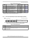
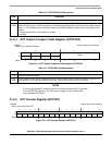
IPSBAR
Offset: 0x1A_000C (GPTIE)
Access: Supervisor read/write
76543210
R 0 0 0 0
CI
W
Reset:00000000
Figure 21-12. GPT Interrupt Enable Register (GPTIE)