


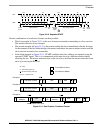

Analog-to-Digital Converter (ADC)
MCF52211 ColdFire® Integrated Microcontroller Reference Manual, Rev. 2
Freescale Semiconductor 26-3
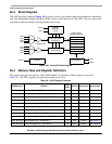
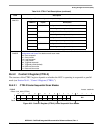
26.4.1 Control 1 Register (CTRL1)
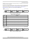
The CTRL1 register, shown in Figure 26-2, is used to configure and control the ADC module. The
associated field descriptions are given in Table 26-2. Please see Section 26.5.6, “Scan Configuration and
Control” for details on the functionality controlled by this register.
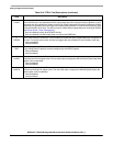
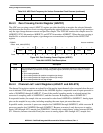
0x19_0032–40 High Limit Registers 0-7 (ADHLMT0-7) 16 R/W 0x0000 26.4.10/26-15
0x19_0042–50 Offset Registers 0-7 (ADOFS0-7) 16 R/W 0x0000 26.4.11/26-17
0x19_0052 Power Control Register (POWER) 16 R/W 0x00D7 26.4.12/26-17
0x19_0054 Voltage Reference Register (CAL) 16 R/W 0x0000 26.4.13/26-20
1
Addresses not assigned to a register and undefined register bits are reserved for expansion.
IPSBAR
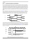
Offset: 0x19_0000 (CTRL1)
Access: read/write
15 14 13 12 11 10 9 8 7 6 5 4 3 2 1 0
R 0
STOP0 SYNC0
EOSI
E0
ZCIE
LLMT
IE
HLMT
IE
CHNCFG SMODE
W
START0
Reset0 1 0 1 00000000 0 1 0 1
Figure 26-2. Control 1 Register (CTRL1)
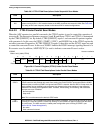
Table 26-2. CTRL1 Field Descriptions
Field Description
15 Reserved, should be cleared.
14
STOP0
Stop Conversion 0 bit. When STOP0 is set, the current scan is stopped and no further scans can start. Any
further SYNC0 input pulses (see the SYNC0 field description) or writes to START0 are ignored until STOP0
is cleared. After the ADC is in stop mode, the result registers can be modified by the processor. Any changes
to the result registers in stop mode are treated as if the analog core supplied the data. Therefore, limit
checking, zero crossing, and associated interrupts can occur if enabled.
0 Normal operation
1 Stop mode
Note: This is not the same as the device’s STOP mode.
13
START0
Start Conversion 0 bit. A scan is started by writing a 1 to this bit. START0 is write-only. Writing 1 to the
START0 bit again is ignored until the end of the current scan. The ADC must be in a stable power
configuration prior to writing to START0 (see Section 26.5.8, “Power Management”).
0 No action
1 Start command is issued
Table 26-1. ADC Register Summary (continued)
IPSBAR Offset
1
Register
Width
(bits)
Access Reset Value Section/Page