


Analog-to-Digital Converter (ADC)
MCF52211 ColdFire® Integrated Microcontroller Reference Manual, Rev. 2
26-2 Freescale Semiconductor
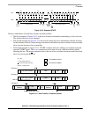
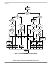
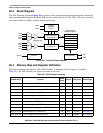
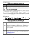
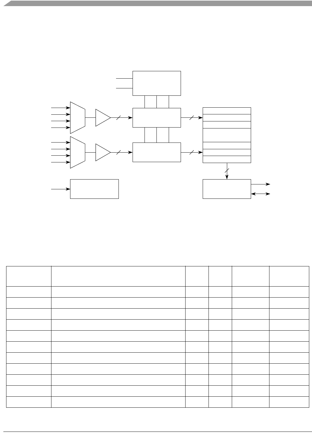
26.3 Block Diagram
The ADC function, shown in Figure 26-1, consists of two four-channel input select functions, interfacing
with two independent Sample and Hold (S/H) circuits, which feed two 12-bit ADCs. The two converters
store their results in a buffer, awaiting further processing.
Figure 26-1. Dual ADC Block Diagram
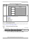
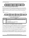
26.4 Memory Map and Register Definition
This section presents the registers of the ADC module. A summary of these registers is given in
Table 26-1. All ADC registers are supervisor-mode access only.
Table 26-1. ADC Register Summary
IPSBAR Offset
1
Register
Width
(bits)
Access Reset Value Section/Page
0x19_0000 Control Register 1 (CTRL1) 16 R/W 0x5005 26.4.1/26-3
0x19_0002 Control Register 2 (CTRL2) 16 R/W 0x0002 26.4.2/26-5
0x19_0004 Zero Crossing Control Register (ADZCC) 16 R/W 0x0000 26.4.3/26-8
0x19_0006 Channel List Register 1 (ADLST1) 16 R/W 0x3210 26.4.4/26-8
0x19_0008 Channel List Register 2 (ADLST2) 16 R/W 0x7654 26.4.4/26-8
0x19_000A Sample Disable Register (ADSDIS) 16 R/W 0x0000 26.4.5/26-10
0x19_000C Status Register (ADSTAT) 16 R/W 0x0000 26.4.6/26-11
0x19_000E Limit Status Register (ADLSTAT) 16 R/W 0x0000 26.4.7/26-13
0x19_0010 Zero Crossing Status Register (ADZCSTAT) 16 R/W 0x0000 26.4.8/26-14
0x19_0012–20 Result Registers 0-7 (ADRSLT0-7) 16 R/W 0x0000 26.4.9/26-14
0x19_0022–30 Low Limit Registers 0-7 (ADLLMT0-7) 16 R/W 0x0000 26.4.10/26-15
IRQ
AN7
AN6
AN5
AN4
Scaling & Cyclic
Converter B
12
AN3
AN2
AN1
AN0
Scaling & Cyclic
Converter A
12
•
•
•
Digital Output
Storage Registers
16
Bus Interface
Data
SYNCx Controller
V
REFH
Voltage
V
REFL
Sample/Hold
Reference
Circuit
MUX
MUX