


Analog-to-Digital Converter (ADC)
MCF52211 ColdFire® Integrated Microcontroller Reference Manual, Rev. 2
26-20 Freescale Semiconductor
26.4.13 Voltage Reference Register (CAL)
In earlier series, this register supported ADC calibration and had a different name. Improvements in ADC
performance have eliminated the need for on-chip calibration support, hence the new name.
1
PD1
Manual Power-Down for Converter B bit. This bit forces Converter B to power-down. Setting PD1
powers-down converter B immediately. The results of a scan using converter B is invalid when PD1 is set.
When PD1 is cleared, converter B is continuously powered-up (APD = 0) or automatically powered-up when
needed (APD = 1).
0 Power-up ADC converter B
1 Power-down ADC converter B
Note: When clearing PD1 in any power mode except auto power-down (APD = 1), wait PUDELAY ADC clock
cycles before initiating a scan to stabilize power levels within the converter. The PSTS1 bit can be
polled to determine when the PUDELAY time has elapsed. Failure to follow this procedure can result
in loss of accuracy of the first two samples.
0
PD0
Manual Power-Down for Converter A bit. This bit forces Converter A to power-down. Setting PD0
powers-down converter A immediately. The results of a scan using converter A is invalid when PD0 is set.
When PD0 is cleared, converter A is continuously powered-up (APD = 0) or automatically powered-up when
needed (APD = 1).
0 = Power-up ADC converter A
1 = Power-down ADC converter A
Note: When clearing PD0 in any power mode except auto power-down (APD = 1), wait PUDELAY ADC clock
cycles before initiating a scan to stabilize power levels within the converter. The PSTS0 bit can be
polled to determine when the PUDELAY time has elapsed. Failure to follow this procedure can result
in loss of accuracy of the first two samples.
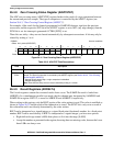
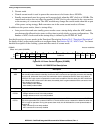
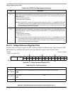
IPSBAR
Offset: 0x19_0054 (CAL)
Access: read/write
15 14 13 12 11 10 9 8 7 6 5 4 3 2 1 0
R
SEL_VREFH SEL_VREFL
0 0 0 00000000000
W
Reset 0 0 00000000000000
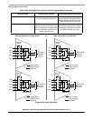
Figure 26-17. Voltage Reference Register (CAL)
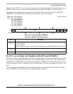
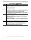
Table 26-19. CAL Field Descriptions
Field Description
15
SEL_VREFH
Select V
REFH
Source bit. This bit selects the source of the V
REFH
reference for conversions.
0VRH
1AN2
14
SEL_VREFL
Select V
REFL
Source bit. This bit selects the source of the V
REFL
reference for conversions.
0VRL
1AN6
13–0 Reserved, should be cleared.
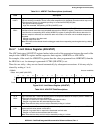
Table 26-18. POWER Field Descriptions (continued)
Field Description