


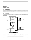
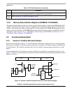

ColdFire Core
MCF52211 ColdFire® Integrated Microcontroller Reference Manual, Rev. 2
3-2 Freescale Semiconductor
instruction, fetches the required operands and then executes the required function. Because the IFP and
OEP pipelines are decoupled by an instruction buffer serving as a FIFO queue, the IFP is able to prefetch
instructions in advance of their actual use by the OEP thereby minimizing time stalled waiting for
instructions.
The V2 ColdFire core pipeline stages include the following:
• Two-stage instruction fetch pipeline (IFP) (plus optional instruction buffer stage)
— Instruction address generation (IAG) — Calculates the next prefetch address
— Instruction fetch cycle (IC)—Initiates prefetch on the processor’s local bus
— Instruction buffer (IB) — Optional buffer stage minimizes fetch latency effects using FIFO
queue
• Two-stage operand execution pipeline (OEP)
— Decode and select/operand fetch cycle (DSOC)—Decodes instructions and fetches the
required components for effective address calculation, or the operand fetch cycle
— Address generation/execute cycle (AGEX)—Calculates operand address or executes the
instruction
When the instruction buffer is empty, opcodes are loaded directly from the IC cycle into the operand
execution pipeline. If the buffer is not empty, the IFP stores the contents of the fetched instruction in the
IB until it is required by the OEP.
For register-to-register and register-to-memory store operations, the instruction passes through both OEP
stages once. For memory-to-register and read-modify-write memory operations, an instruction is
effectively staged through the OEP twice: the first time to calculate the effective address and initiate the
operand fetch on the processor’s local bus, and the second time to complete the operand reference and
perform the required function defined by the instruction.
The resulting pipeline and local bus structure allow the V2 ColdFire core to deliver sustained high
performance across a variety of demanding embedded applications.
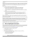
3.2 Memory Map/Register Description
The following sections describe the processor registers in the user and supervisor programming models.
The programming model is selected based on the processor privilege level (user mode or supervisor mode)
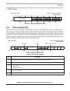
as defined by the S bit of the status register (SR). Table 3-1 lists the processor registers.
The user-programming model consists of the following registers:
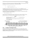
• 16 general-purpose 32-bit registers (D0–D7, A0–A7)
• 32-bit program counter (PC)
• 8-bit condition code register (CCR)
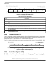
• MAC registers (described fully in Chapter 4, “Multiply-Accumulate Unit (MAC)”):
— One 32-bit accumulator(ACC) register
— One 16-bit mask register (MASK)
— 8-bit Status register (MACSR)