


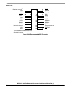
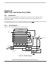


IEEE 1149.1 Test Access Port (JTAG)
MCF52211 ColdFire® Integrated Microcontroller Reference Manual, Rev. 2
29-2 Freescale Semiconductor
29.1.2 Features
The basic features of the JTAG module are the following:
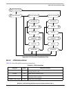
• Performs boundary-scan operations to test circuit board electrical continuity
• Bypasses instruction to reduce the shift register path to a single cell
• Sets chip output pins to safety states while executing the bypass instruction
• Samples the system pins during operation and transparently shifts out the result
• Selects between JTAG TAP controller and Background Debug Module (BDM) using a dedicated
JTAG_EN pin
29.1.3 Modes of Operation
The JTAG_EN pin can select between the following modes of operation:
• JTAG mode (JTAG_EN = 1)
• Background debug mode (BDM)—for more information, refer to Section 28.5, “Background
Debug Mode (BDM)”; (JTAG_EN = 0).
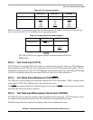
29.2 External Signal Description
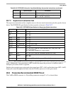
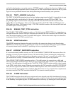
The JTAG module has five input and one output external signals, as described in Table 29-1.
29.2.1 JTAG Enable (JTAG_EN)
The JTAG_EN pin selects between the debug module and JTAG. If JTAG_EN is low, the debug module is
selected; if it is high, the JTAG is selected. Table 29-2 summarizes the pin function selected depending on
JTAG_EN logic state.
Table 29-1. Signal Properties
Name Direction Function Reset State Pull up
JTAG_EN Input JTAG/BDM selector input — —
TCLK Input JTAG Test clock input — Active
TMS/BKPT Input JTAG Test mode select / BDM Breakpoint — Active
TDI/DSI Input JTAG Test data input / BDM Development serial input — Active
TRST/DSCLK Input JTAG Test reset input / BDM Development serial clock — Active
TDO/DSO Output JTAG Test data output / BDM Development serial output Hi-Z / 0 —