


Queued Serial Peripheral Interface (QSPI)
MCF52211 ColdFire® Integrated Microcontroller Reference Manual, Rev. 2
Freescale Semiconductor 23-11
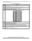
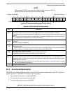
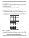
23.4.1 QSPI RAM
The QSPI contains an 80-byte block of static RAM that can be accessed by the user and the QSPI. This
RAM does not appear in the device memory map, because it can only be accessed by the user indirectly
through the QSPI address register (QAR) and the QSPI data register (QDR). The RAM is divided into
three segments with 16 addresses each:
• Receive data RAM—the initial destination for all incoming data
• Transmit data RAM—a buffer for all out-bound data
• Command RAM—where commands are loaded
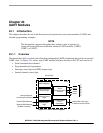
The transmit and command RAM are user write-only. The receive RAM is user read-only. Figure 23-10
shows the RAM configuration. The RAM contents are undefined immediately after a reset.
The command and data RAM in the QSPI is indirectly accessible with QDR and QAR as 48 separate
locations that comprise 16 words of transmit data, 16 words of receive data, and 16 bytes of commands.
A write to QDR causes data to be written to the RAM entry specified by QAR[ADDR] and causes the
value in QAR to increment. Correspondingly, a read at QDR returns the data in the RAM at the address
specified by QAR[ADDR]. This also causes QAR to increment. A read access requires a single wait state.
23.4.1.1 Receive RAM
Data received by the QSPI is stored in the receive RAM segment located at 0x10 to 0x1F in the QSPI RAM
space. The user reads this segment to retrieve data from the QSPI. Data words with less than 16 bits are
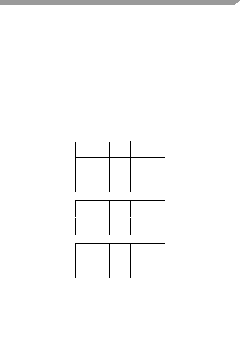
Relative
Address
Register Function
0x00 QTR0 Transmit RAM
0x01 QTR1
... ... 16 bits wide
0x0F QTR15
0x10 QRR0 Receive RAM
0x11 QRR1
... ... 16 bits wide
0x1F QRR15
0x20 QCR0 Command RAM
0x21 QCR1
... ... 8 bits wide
0x2F QCR15
Figure 23-10. QSPI RAM Model