


EM78P259N/260N
8-Bit Microprocessor with OTP ROM
Product Specification (V1.2) 05.18.2007
• 5
(This specification is subject to change without further notice)
6 Function Description
6.1 Operational Registers
6.1.1 R0 (Indirect Address Register)
R0 is not a physically implemented register. Its major function is to perform as an
indirect address pointer. Any instruction using R0 as a pointer, actually accesses the
data pointed by the RAM Select Register (R4).
6.1.2 R1 (Time Clock /Counter)
Increased by an external signal edge which is defined by the TE bit (CONT-4)
through the TCC pin, or by the instruction cycle clock.
Writable and readable as any other registers
The TCC prescaler counter (IOCC1) is assigned to TCC
The contents of the IOCC1 register is cleared –
• when a value is written to the TCC register.
• when a value is written to the TCC prescaler bits (Bits 3, 2, 1, 0 of the CONT
register)
• during power-on reset, /RESET, or WDT time out reset.
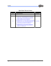
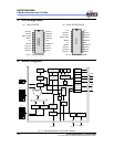
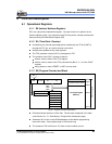
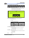
6.1.3 R2 (Program Counter) and Stack
A7 ~ A0
On-chip Program
Memory
000H
7FFH
003H
Hardware Interrupt Vector
User Memory Space
Reset Vector
A9 A8 A10
Stack Level 1
Stack Level 3
Stack Level 2
Stack Level 4
Stack Level 5
CALL
00 PAGE0 0000~03FF
01 PAGE1 0400~07FF
R3
RET
RETL
RETI
Stack Level 6
Stack Level 7
Stack Level 8
01EH
~
3FEH
Fig. 6-1 Program Counter Organization
R2 and hardware stacks are 12-bit wide. The structure is depicted in the table
under Section 6.1.3.1, Data Memory Configuration (subsequent page).
Generates 2K×13 bits on-chip ROM addresses to the relative programming
instruction codes. One program page is 1024 words long.
The contents of R2 are all set to "0"s when a reset condition occurs.