


EM78P259N/260N
8-Bit Microprocessor with OTP ROM
Product Specification (V1.2) 05.18.2007
• 15
(This specification is subject to change without further notice)
6.2 Special Purpose Registers
6.2.1 A (Accumulator)
Internal data transfer operation, or instruction operand holding usually involves the
temporary storage function of the Accumulator, which is not an addressable register.
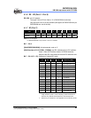
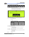
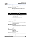
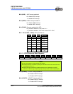
6.2.2 CONT (Control Register)
Bit 7 Bit 6 Bit 5 Bit 4 Bit 3 Bit 2 Bit 1 Bit 0
INTE INT TS TE PSTE PST2 PST1 PST0
Note: The CONT register is both readable and writable
Bit 6 is read only.
Bit 7 (INTE): INT signal edge
0 = interrupt occurs at the rising edge on the INT pin
1 = interrupt occurs at the falling edge on the INT pin
Bit 6 (INT): Interrupt enable flag
0 = masked by DISI or hardware interrupt
1 = enabled by the ENI/RETI instructions
This bit is readable only.
Bit 5 (TS): TCC signal source
0 = internal instruction cycle clock. P54 is bi-directional I/O pin.
1 = transition on the TCC pin
Bit 4 (TE): TCC signal edge
0 = increment if the transition from low to high takes place on the TCC
pin
1 = increment if the transition from high to low takes place on the TCC
pin.
Bit 3 (PSTE): Prescaler enable bit for TCC
0 = prescaler disable bit. TCC rate is 1:1.
1 = prescaler enable bit. TCC rate is set as Bit 2 ~ Bit 0.