


EM78P259N/260N
8-Bit Microprocessor with OTP ROM
Product Specification (V1.2) 05.18.2007
• 21
(This specification is subject to change without further notice)
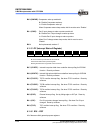
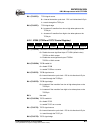
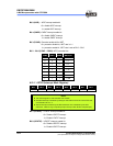
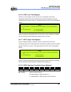
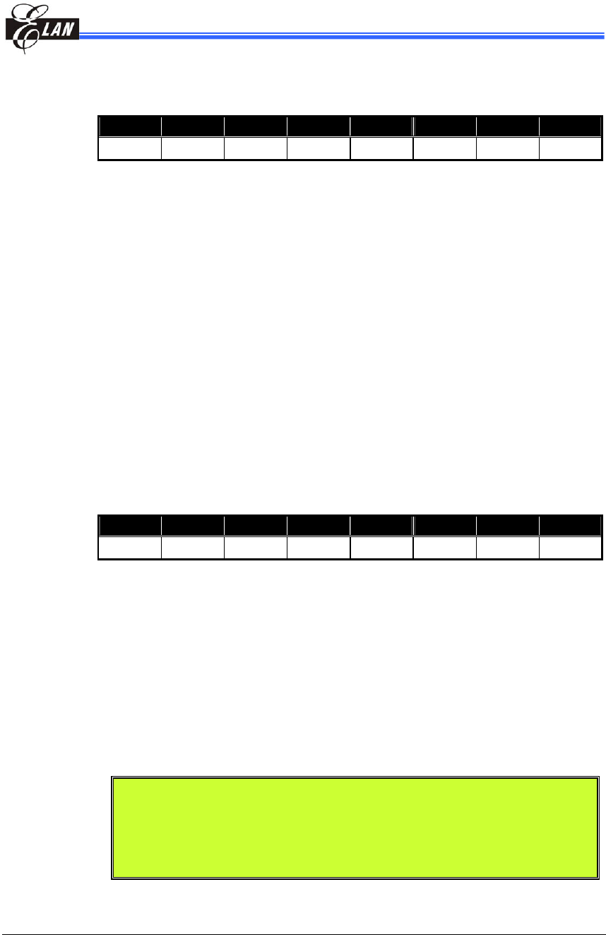
6.2.9 IOCD0 (Pull-high Control Register)
Bit 7 Bit 6 Bit 5 Bit 4 Bit 3 Bit 2 Bit 1 Bit 0
/PH57 /PH56 /PH55 /PH54 /PH53 /PH52 /PH51 /PH50
Note: The IOCD0 register is both readable and writable
Bit 7 (/PH57): Control bit is used to enable the pull-high of the P57 pin (applicable to
EM78P260N only).
0 = Enable internal pull-high;
1 = Disable internal pull-high.
Bit 6 (/PH56): Control bit used to enable the pull-high function of the P56 pin
(applicable to EM78P260N only).
Bit 5 (/PH55): Control bit used to enable the pull-high function of the P55 pin.
Bit 4 (/PH54): Control bit used to enable the pull-high function of the P54 pin.
Bit 3 (/PH53): Control bit used to enable the pull-high function of the P53 pin.
Bit 2 (/PH52): Control bit used to enable the pull-high function of the P52 pin.
Bit 1 (/PH51): Control bit used to enable the pull-high function of the P51 pin.
Bit 0 (/PH50): Control bit used to enable the pull-high function of the P50 pin.
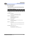
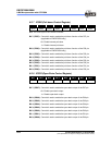
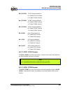
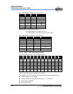
6.2.10 IOCE0 (WDT Control & Interrupt Mask Registers 2)
Bit 7 Bit 6 Bit 5 Bit 4 Bit 3 Bit 2 Bit 1 Bit 0
WDTE EIS ADIE CMPIE PSWE PSW2 PSW1 PSW0
Bit 7 (WDTE): Control bit used to enable Watchdog Timer
0 = Disable WDT
1 = Enable WDT
WDTE is both readable and writable
Bit 6 (EIS): Control bit used to define the function of the P60 (/INT) pin
0 = P60, bi-directional I/O pin
1 = /INT, external interrupt pin. In this case, the I/O control bit of P60
(Bit 0 of IOC60) must be set to "1"
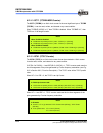
NOTE
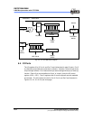
■ When EIS is "0," the path of /INT is masked. When EIS is "1," the status of /INT pin
can also be read by way of reading Port 6 (R6). Refer to Fig. 6-4 (I/O Port and I/O
Control Register Circuit for P60 (/INT)) under Section 6.4 (I/O Ports).
■ EIS is both readable and writable.