


EM78P259N/260N
8-Bit Microprocessor with OTP ROM
Product Specification (V1.2) 05.18.2007
• 3
(This specification is subject to change without further notice)
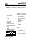
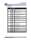
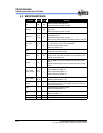
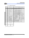
5 Pin Description
5.1 EM78P259NP/M
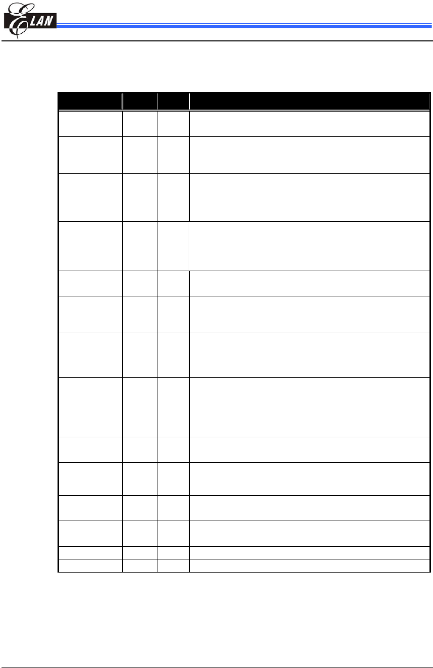
Symbol Pin No. Type Function
P70 15 I/O
General purpose input/output pin
Default value after a power-on reset
P60~P67 6~13 I/O
General purpose input/output pin
Open-drain
Default value after a power-on reset
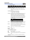
P50~P55
1~3
16~18
I/O
General purpose input/output pin
Pull-high/pull-down
Default value after a power-on reset
Wake up from sleep mode when the status of the pin changes
CIN-, CIN+
CO
12, 11
10
I
O
“-“ : the input pin of Vin- of the comparator
“+” : the input pin of Vin+ of the comparator
Pin CO is the comparator output
Defined by IOC80 <4:3>
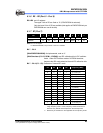
OSCI 16 I
Crystal type: Crystal input terminal or external clock input pin
RC type: RC oscillator input pin
OSCO 15 I/O
Crystal type: Crystal input terminal or external clock input pin.
RC type: clock output with a duration of one instruction cycle
External clock signal input
/RESET 4 I
If set as /RESET and remains at logic low, the device will be
reset
Voltage on /RESET/Vpp must not exceed Vdd during normal
mode
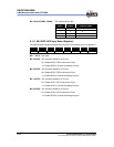
TCC, TCCA,
TCCB, TCCC
3, 7,
8, 9
I
External Counter input
TCC is defined by CONT <5>
TCCA is defined by IOC80 <1>
TCCB is defined by IOC90 <5>
TCCC is defined by IOC90 <1>
ADC0~ADC3
1, 2,
17, 18
I
Analog to Digital Converter
Defined by ADCON (R9) <1:0>
IR OUT 13 O
IR mode output pin, capable of driving and sinking
current=20mA when the output voltage drops to 0.7Vdd and
rise to0.3Vdd at Vdd=5V.
VREF 3 I
External reference voltage for ADC
Defined by ADCON (R9) <7>
/INT 6 I
External interrupt pin triggered by a falling or rising edge
Defined by CONT <7>
VDD 14 – Power supply
VSS 5 – Ground