


EM78P259N/260N
8-Bit Microprocessor with OTP ROM
44 •
Product Specification (V1.2) 05.18.2007
(This specification is subject to change without further notice)
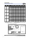
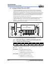
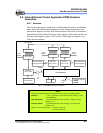
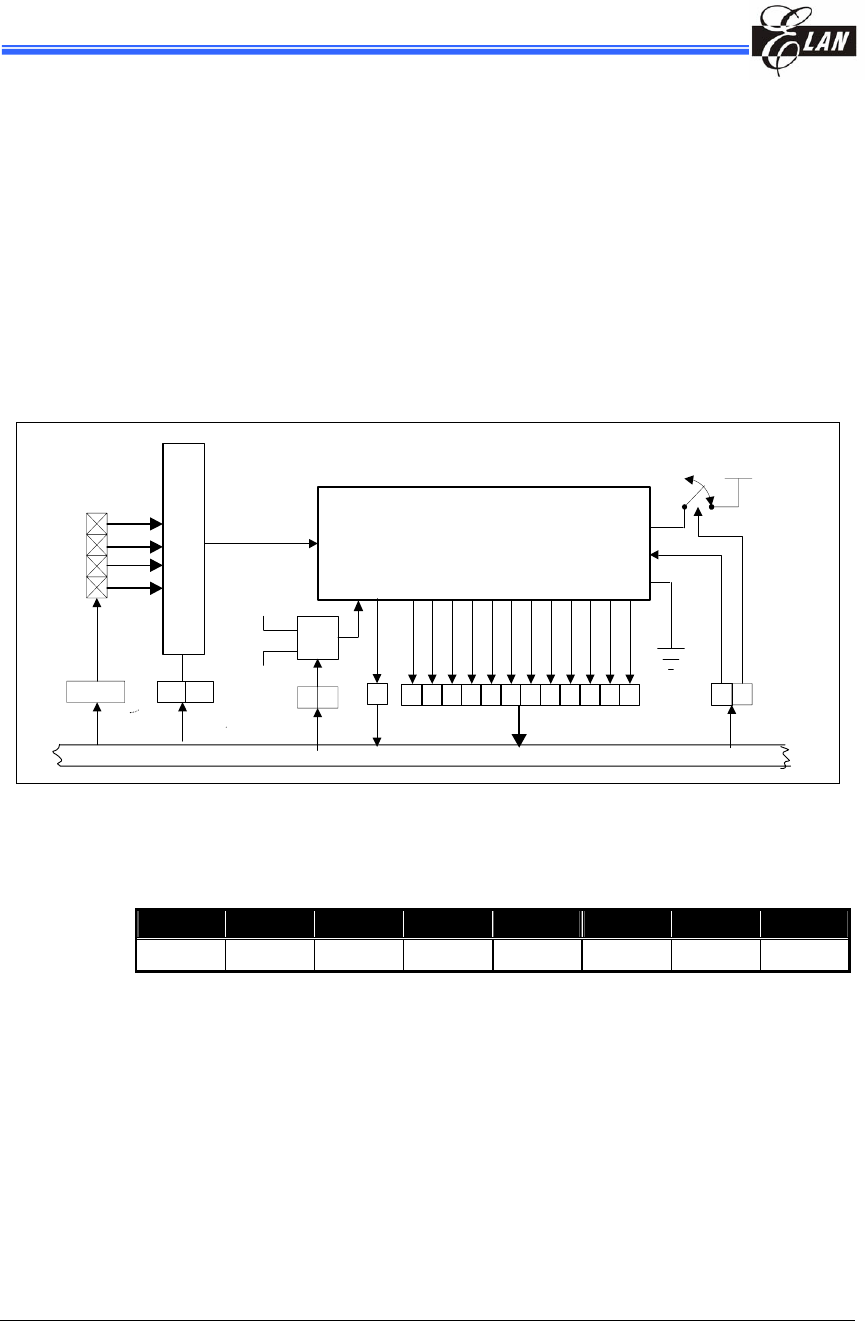
6.7 Analog-to-Digital Converter (ADC)
The analog-to-digital circuitry consist of a 4-bit analog multiplexer; three control
registers (AISR/R8, ADCON/R9, & ADOC/RA), three data registers (ADDATA/RB,
ADDATA1H/RC, & ADDATA1L/RD), and an ADC with 12-bit resolution as shown in the
functional block diagram below. The analog reference voltage (Vref) and the analog
ground are connected via separate input pins. Connecting to the external VREF is
more accurate than connecting to the internal VDD.
The ADC module utilizes successive approximation to convert the unknown analog
signal into a digital value. The result is fed to the ADDATA, ADDATA1H, and
ADDATA1L. Input channels are selected by the analog input multiplexer via the
ADCON register Bits ADIS1 and ADIS0.
ADDATA1H
DATA BUS
ADC3
ADC2
ADC1
ADC0
Vref
Power-Down
Fsco
Internal RC
4-1
MUX
7 ~ 0
34
ADC
( successive approximation )
3
56
ADCON RF
AISR
ADCON
Start to Convert
01
ADCON
8-1 Analog Switch
01234567891011
ADDATA1L
Fig. 6-10 Analog-to-Digital Conversion Functional Block Diagram
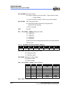
6.7.1 ADC Control Register (AISR/R8, ADCON/R9, ADOC/RA)
6.7.1.1 R8 (AISR: ADC Input Select Register)
Bit 7 Bit 6 Bit 5 Bit 4 Bit 3 Bit 2 Bit 1 Bit 0
– – – – ADE3 ADE2 ADE1 ADE0
The AISR register individually defines the Port 5 pins as analog input or as digital I/O.
Bit 7 ~ 4: Not used
Bit 3 (ADE3): AD converter enable bit of P53 pin
0 = Disable ADC3, P53 acts as I/O pin
1 = Enable ADC3 acts as analog input pin
Bit 2 (ADE2): AD converter enable bit of P52 pin
0 = Disable ADC2, P53 acts as I/O pin
1 = Enable ADC2 acts as analog input pin