


EM78P259N/260N
8-Bit Microprocessor with OTP ROM
Product Specification (V1.2) 05.18.2007
• 45
(This specification is subject to change without further notice)
Bit 1 (ADE1): AD converter enable bit of P51 pin
0 = Disable ADC1, P51 acts as I/O pin
1 = Enable ADC1 acts as analog input pin
Bit 0 (ADE0): AD converter enable bit of P50 pin
0 = Disable ADC0, P50 acts as I/O pin
1 = Enable ADC0 acts as analog input pin
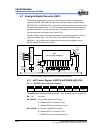
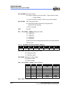
6.7.1.2 R9 (ADCON: AD Control Register)
Bit 7 Bit 6 Bit 5 Bit 4 Bit 3 Bit 2 Bit 1 Bit 0
VREFS CKR1 CKR0 ADRUN ADPD - ADIS1 ADIS0
The ADCON register controls the operation of the AD conversion and determines
which pin should be currently active.
Bit 7(VREFS): Input source of the ADC Vref
0 = The ADC Vref is connected to Vdd (default value), and the
P54/VREF pin carries out the P54 function
1 = The ADC Vref is connected to P54/VREF
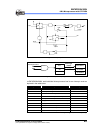
NOTE
The P54/TCC/VREF pin cannot be applied to TCC and VREF at the same time. IF
P54/TCC/VREF acts as VREF analog input pin, then CONT Bit 5 (TS) must be “0”.
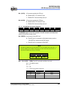
The P54/TCC/VREF pin priority is as follows:
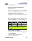
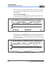
Bit 6 ~ Bit 5 (CKR1 ~ CKR0): The ADC prescaler oscillator clock rate
00 = 1: 16 (default value)
01 = 1: 4
10 = 1: 64
11 = 1: WDT ring oscillator frequency
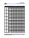
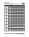
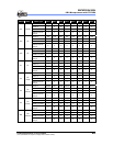
CKR1:CKR0 Operation Mode Max. Operation Frequency
00 Fosc/16 4 MHz
01 Fosc/4 1 MHz
10 Fosc/64 16 MHz
11 Internal RC –
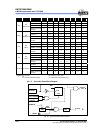
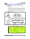
P54/TCC/VREF Pin Priority
High Medium Low
VREF TCC P54