


EM78P259N/260N
8-Bit Microprocessor with OTP ROM
Product Specification (V1.2) 05.18.2007
• 11
(This specification is subject to change without further notice)
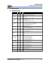
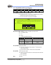
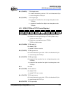
6.1.9 R9 (ADCON: ADC Control Register)
Bit 7 Bit 6 Bit 5 Bit 4 Bit 3 Bit 2 Bit 1 Bit 0
VREFS CKR1 CKR0 ADRUN ADPD – ADIS1 ADIS0
Bit 7 (VREFS): Input source of the Vref of the ADC
0 = The Vref of the ADC is connected to Vdd (default value), and the
P54/VREF pin carries out the function of P54
1 = The Vref of the ADC is connected to P54/VREF
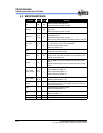
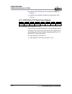
NOTE
The P54/TCC/VREF pin cannot be applied to TCC and VREF at the same time.
If P54/TCC/VREF functions as VREF analog input pin, then CONT Bit 5 “TS”
must be “0.”
The P54/TCC/VREF pin priority is as follows:
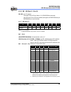
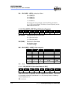
Bit 6 & Bit 5 (CKR1 & CKR0): Prescaler of oscillator clock rate of ADC
00 = 1: 16 (default value)
01 = 1: 4
10 = 1: 64
11 = 1: WDT ring oscillator frequency
CKR1:CKR0 Operation Mode Max. Operation Frequency
00 Fosc/16 4 MHz
01 Fosc/4 1 MHz
10 Fosc/64 16 MHz
11 Internal RC –
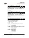
Bit 4 (ADRUN): ADC starts to RUN.
0 = Reset upon completion of the conversion. This bit cannot be
reset through software
1 = AD conversion is started. This bit can be set by software.
Bit 3 (ADPD): ADC Power-down mode
0 = Switch off the resistor reference to conserve power even while the
CPU is operating
1 = ADC is operating
Bit 2: Not used
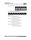
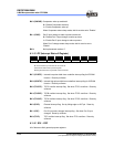
P53/TCC/VREF Pin Priority
High Medium Low
VREF TCC P54