


10/100 Mbps Ethernet Controller Family Open Source Software Developer Manual 129
Physical Layer Interface
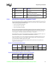
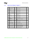
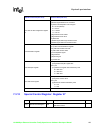
7.3.12 Special Control Register: Register 27
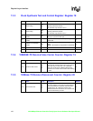
011 Write to ASD configuration register
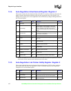
2
[9] Breakdown ASD counters.
[8] Selects signal detections or transitions.
[7:6] Slow mode adaptation time configure:
00 = 67 ms (default)
01 = 0.5 ms
10 = 16.8 ms
11 = 134 ms
[5] Signal detect force enable.
[4] Signal detect force value.
[3:2] Reserved.
[1] Disable signal detect high threshold value.
[0] Disable signal detect low threshold value.
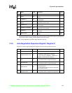
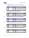
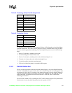
100 Read status register
[15:14] Reserved.
[13:11] ASD command/address register.
[10:9] TMD100 transition ratio bits.
[8:7] ASD state machine state.
[6] Lock adaptation signal.
[5] Signal detect.
[4] Squelch signal.
[3:0] Coded zero.
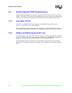
101 Read jitter register
Read cycle:
[15:0] Reflects the jitter register bits.
Write cycle:
[1:0] Selects the register lines reflected by read.
00 = Bits 15:0
01 = Bits 21:6
1x = Bits 26:11
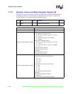
110 Read clock register
Read cycle:
[15:0] Clock counter value.
Write cycle:
[0] Selects the window reflected by read.
0 = 15:0
1 = 23:8
111 Reserved
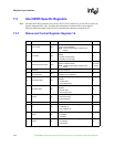
Bit Name R / W Description Default
15:0 Special Control Register RW
Bits 15:3 are reserved, and bits 2:0 are used for the
LED switch control.
Opcode Command (bits 15:13) Command Data (bits 12:0)