


16 Intel 8255x 10/100 Mbps Ethernet Controller Family Open Source Software Developer Manual
PCI Interface
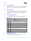
The 8255x requires one BAR for I/O mapping and one BAR for memory mapping of these
registers anywhere within the 32-bit memory address space. The driver determines which BAR (I/
O or Memory) is used to access the Control/Status Registers. However, both are always requested
by the device.
One BAR is also required to map the accesses to an optional Flash memory. The 82557 implements
this register regardless of the presence or absence of a Flash chip on the adapter. The 82558 and
82559 only implement this register if a bit is set in the EEPROM. The size of the space requested
by this register is 1Mbyte, and it is always mapped anywhere in the 32-bit memory address space.
Note: Although the 82558 only supports up to 64 Kbytes of Flash memory and the 82559 only supports
128 Kbytes of Flash memory, 1 Mbyte of address space is still requested. Software should not
access Flash addresses above 64 Kbytes for the 82558 or 128 Kbytes for the 82559 because Flash
accesses above the limits are aliased to lower addresses. Table 3 describes the implementation of
the base address registers.
4.1.11 Subsystem ID (Offset 2C)
This register uniquely identifies the add-in adapter or subsystem where the PCI device resides. It
provides a mechanism to distinguish different adapters that use the same PCI controller. For the
82557 B-step this field equals 0000h. For the 82557 C-Step and later devices, this field is loaded
from the EEPROM at power on or upon the assertion of PCI reset. If the EEPROM is not present or
invalid, this value defaults to 0000h.
4.1.12 Subsystem Vendor ID (Offset 2E)
This register uniquely identifies the add-in adapter or subsystem where the PCI device resides. It
provides a mechanism to distinguish the vendor of a adapter from the vendor of the PCI controller
used on the adapter. For the 82557 B-step this field is 0000h. For the 82557 C-Step and later
devices, this field is automatically loaded from the EEPROM at power on or upon the assertion of
PCI reset. If the EEPROM is not present or invalid, this value defaults to 0000h.
4.1.13 Expansion ROM Base Address Register (Offset 30)
The 8255x provides an interface to a local Flash device (or EEPROM) which may be used as an
expansion ROM. A 32-bit Expansion ROM Base Address Register at offset 30h in the PCI
Configuration Space is defined to handle the address and size information for boot-time access to
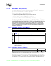
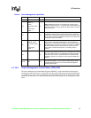
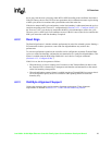
Table 3. Base Address Register Summary
Register
Location
Description
10h
Memory space for the device Control/Status Registers. The size of this space is 4 Kbytes
and it is mapped anywhere in the 32-bit memory address space. It is marked as pre-
fetchable. Software should not assume that this memory will be granted below 1 Mbyte.
14h I/O space for the device Control/Status Registers. The size of this space is 32 bytes.
18h
Memory space for FLASH buffer accesses. The size of this space is 1Mbyte. It is mapped
anywhere in the 32-bit address space and is not pre-fetchable.
1Ch - 27h Reserved.