


Intel 8255x 10/100 Mbps Ethernet Controller Family Open Source Software Developer Manual 49
Host Software Interface
6.3.4.4 Software Write Access to the EEPROM
Write access to the EEPROM is similar to the read access outlined above, with the differences of a
write opcode and step 4:
1. Activate the EEPROM by writing a 1 to the EECS bit.
2. Write the read opcode, including the start bit (110b), one bit at a time, starting with the most
significant bit (1):
a. Write the opcode bit to the EEDI bit.
b. Write a 1 to EESK bit then wait the minimum SK high time.
c. Write a 0 to EESK bit then wait the minimum SK low time.
d. Repeat steps 2.a through 2.c for the next two opcode bits.
3. Write the address field, one bit at a time, starting with the most significant bit.
a. Write the address bit to the EEDI bit.
b. Write a 1 to EESK bit then wait the minimum SK high time.
c. Write a 0 to EESK bit then wait the minimum SK low time.
d. Read the EEDO bit (looking for the dummy 0 bit).
e. Repeat steps 3.a through 3.d until the EEDO bit equals 0, indicating that the address field
has been completely written.
4. Write a 16-bit word to the EEPROM, one bit at a time, starting with the most significant bit
(write a data bit to the EEDI bit):
a. Write a 1 to the EESK bit then wait the minimum SK high time.
b. Write a 0 to the EESK bit then wait the minimum SK low time.
c. Repeat steps 4.a through 4.c an additional 15 times.
5. De-activate the EEPROM by writing a 0 to the EECS bit.
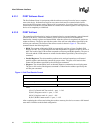
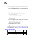
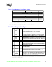
6.3.5 Management Data Interface Control Register
The Management Data Interface (MDI) Control register is a 32-bit entity at offset 10h of the CSR.
The MDI Control register is used to read and write bits from the management data Interface. More
details regarding the MDI can be found in Section 7.1, “Management Data Interface (MDI)” and
Section 8.1.2, “PHY Detection and Initialization”.
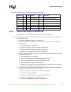
Table 24. MDI Control Register Location
Upper Word (D31:D16) Lower Word (D15:D0) Offset
SCB Command Word SCB Status Word Base + 0h
SCB General Pointer Base + 4h
PORT Base + 8h
EEPROM Control Register Reserved Base + Ch
MDI Control Register Base + 10h