


Intel 8255x 10/100 Mbps Ethernet Controller Family Open Source Software Developer Manual 69
Host Software Interface
systems that are extremely cache line oriented. More information of the read alignment
capability is detailed in Section 4.2.2, “Read Align”.
0 = Read Alignment disabled.
1 = Read Alignment enabled.
Default - 0 (Read Alignment disabled).
Recommended - 0.
— Bit 0 - MWI Enable. This bit is reserved on the 82557 and should be set to 0.
However, for the 82558 and later generation controllers, it enables the device to perform
Memory Write and Invalidate (MWI) cycles on the PCI bus. If both this bit and the MWI
enable bit in the PCI command register are both set, then the device attempts to perform
MWI cycles when writing data to system memory. If either this bit or the MWI enable bit
in the PCI command register are clear, the device will not perform MWI cycles. A more
detailed description of MWI can be found in Section 4.2.1, “Memory Write and
Invalidate”.
0 = MWI disabled. The device will not perform MWI cycles even if it is permitted by the
PCI command register.
1 = MWI enabled. The device will perform MWI cycles if it is permitted by the PCI
command register.
Default - 0 (MWI disabled).
Recommended - 1.
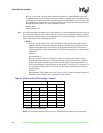
• BYTE 4.
Bits 6:0 - Receive DMA Maximum Byte Count. This byte indicates the maximum number of
receive DMA PCI transfers that will be completed before internal arbitration. The counter has
a 4 cycle resolution. This counter is useful in throttling back the receive DMA in order to let
other device DMA channels, such as the transmit DMA, CU DMA, or RU DMA, complete
PCI cycles. For instance, if the counter is set to 4, the receive DMA will only do a 16-cycle
PCI transfer if one of the other internal DMA channels also wants to initiate a transfer. If no
other internal DMA channels are requesting a transfer, the receive DMA may run an extended
PCI burst. In order for this counter to be enabled, the DMA maximum byte count enable bit
(byte 5, bit 7) must be set. If the enable bit is not set, the receive DMA will continue until it is
finished (no other DMA unit can pre-empt it).
Note: If this counter is enabled and set to zero, then the receive DMA may be pre-empted
almost immediately.
Default - 0.
Recommended - 0.
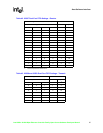
• BYTE 5.
— Bit 7 - DMA Maximum Byte Count Enable. Bit 7 enables the receive and transmit DMA
maximum byte count enable counters. These counters are only valid when this bit is set to
1. This bit enables both the receive and transmit DMA maximum byte counters.
Default - 0.
Recommended - 0.
— Bit 6:0 - Transmit DMA Maximum Byte Count. This byte indicates the maximum number
of transmit DMA PCI cycles that will be completed after internal arbitration. The counter
has a 4 cycle resolution. It is useful in throttling back the transmit DMA in order to let
other DMA channels, such as the receive DMA, CU DMA, or RU DMA complete PCI
cycles. For instance, if the counter is set to 4, the transmit DMA will only do a 16-cycle
PCI transfer if one of the other internal DMA channels also wants to initiate a transfer. If