


Intel 8255x 10/100 Mbps Ethernet Controller Family Open Source Software Developer Manual 17
PCI Interface
the Flash. The 82557 implements this register regardless of the presence or absence of a Flash
component on the adapter. For the 82558 and later Fast Ethernet controllers, this register is only
implemented if a bit is set in the EEPROM.
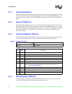
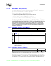
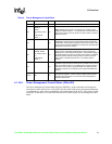
The register functions exactly like a 32-bit base address register except that the encoding (and
usage) of the bottom bits is different. The upper 21 bits correspond to the upper 21 bits of the
expansion ROM base address. The 8255x only allow an expansion ROM to be mapped on a 1
Mbyte boundary. Therefore, only the most significant 12 bits are configurable to indicate the 1
Mbyte size requirement (as with the Flash Memory Mapped BAR, the 82558 and 82559 request a 1
Mbyte mapping even though the maximum Flash size allowed with those devices is 65 Kbytes).
The format of the register is shown in the figure below.
Bit 0 in the register is used to control whether or not the device accepts accesses to its expansion
ROM. When this bit is reset, the devices expansion ROM address space is disabled. This bit is
programmed at initialization time by the system BIOS. The Memory Space bit in the Command
register has precedence over the Expansion ROM Base Address Enable bit. A device responds to
accesses to its expansion ROM only if both the Memory Space bit and the Expansion ROM Base
Address Enable bit are set to 1 (it is reset to 0 upon PCI reset).
4.1.14 The Capabilities Pointer (Offset 34)
This an 8-bit field that provides an offset in the device PCI Configuration Space for the location of
the first item in the Capabilities Linked List. The Power Management Interface documentation
specifies this linked list to provide access to all appropriate device information in the
implementation of the ACPI.
For the 82257, this register is hard-wired to 0 since it does not support power management.
For the 82558 this register is set to DCh if power management is enabled in the EEPROM. If power
management is disabled, then this register is set to 0.
For the 82559 and later Intel Fast Ethernet controllers, this register is hard-wired to DCh.
4.1.15 Interrupt Line (Offset 3C)
The Interrupt Line register is an 8-bit register used to communicate interrupt line routing
information. This register is configurable by the system BIOS or OS. POST software writes the
routing information into this register as it initializes and configures the system. The value in this
register specifies which system interrupt controller input the device interrupt pin is connected to.
Device drivers and operating systems use this information to determine priority and vector
information.
4.1.16 Interrupt Pin (Offset 3D)
The Interrupt Pin register specifies which interrupt pin the device (or device function) uses. This
register is always set to a 1, indicating that INTA# is used.
Figure 7. Expansion ROM Base Address Register
32 20 19 1 0
Read / Write Reserved (all bits set to 0) En