


Intel 8255x 10/100 Mbps Ethernet Controller Family Open Source Software Developer Manual 15
PCI Interface
4.1.10 Built in Self Test (Offset F)
This optional register is used for control and status of Built in Self Test (BIST). This register is
hard-wired to 0 indicating that the devices do not support BIST.
Three base address registers are supported by the 8255x:
• CSR Memory Mapped Base Address Register (BAR 0 at offset 10)
• CSR I/O Mapped Base Address Register (BAR 1 at offset 14)
• Flash Memory Mapped Base Address Register (BAR 2 at offset 18)
Two request memory mapped resources, and the third, I/O mapping. Each register is 32 bits wide.
The least significant bit in each base address register determines whether it represents an I/O or
memory space. The figures below illustrate layouts for I/O and memory mapped base address
registers. After determining which resources will be used, the power-up software maps the I/O and
memory controllers into available locations and continues with the power up. To perform the
mapping in a device independent manner, the base registers are placed in the predefined header
portion of configuration space. Device drivers access this configuration space to determine the
mapping of a particular device.
NOTE: Bit 0 in all base registers is read-only and used to determine whether the register maps into memory or
I/O space. Base registers mapping to memory space must return a 0 in bit 0, and base registers
mapping to I/O space, a 1.
NOTE: Base registers that map into I/O space are always 32 bits with bit 0 hard wired to a 1, bit 1 is reserved
and must return 0 on reads, and the other bits are used to map the device into I/O space.
The number of upper bits that a device actually implements depends on how much of the address
space the device responds to. A device that wants a 1 Mbyte memory address space would set the
most significant 12 bits of the base address register to be configurable, setting the other bits to 0.
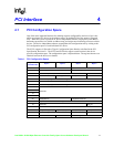
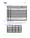
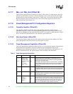
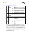
Figure 5. Base Address Register for Memory Mapping
32 43 0
Base Address Configuration Bits
Bits
Initial
Value
Description
31:4 x Base Address.
3 x Pre-fetchable.
2:1 x
00 = Locate address anywhere in 32-bit address space.
01 = Locate address below 1 MByte.
10 = Locate address anywhere in 64-bit address space.
11 = Reserved.
0 0 Memory space indicator.
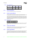
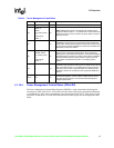
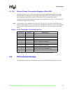
Figure 6. Base Address Register for I/O Mapping
32 21 0
Base Address Reserved 1