


50 Intel 8255x 10/100 Mbps Ethernet Controller Family Open Source Software Developer Manual
Host Software Interface
The MII Management Interface allows software to have direct control over a MII compatible PHY
through a control register in the device. This allows the driver software to place the PHY in specific
modes such as full duplex, loopback, power down, etc., without the need for specific hardware pins
to select the desired mode. This register, called the MDI Control register, resides at offset 10h in
the Control register block. The CPU writes commands to this register and the Ethernet controller
reads or writes control and status parameters to the PHY device through a serial, bi-directional data
pin called Management Data Input/Output (MDIO). These serial data transfers are clocked by the
management data clock output from the LAN controller.
6.3.5.1 MDI Control Register
The MDI register may be written as a 32-bit entity, two 16-bit entities, or four 8-bit entities. When
writing to the MDI register using word or byte access, the data is latched only on the write to the
most significant byte of the register, which is located at offset 13h. Thus, the high byte should be
written last.
6.3.5.2 MDI Write cycle
The sequence of events for a MDI write cycle is:
1. The CPU performs a PCI write cycle to the MDI register with:
a. Ready (bit 28) = 0
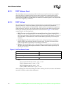
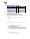
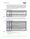
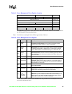
Table 25. Management Data Pins
Symbol Type Name and Function
MDIO In/Out
Management Data Input/Output. MDIO is a bi-directional signal between the device
and an MII compatible PHY. It is used to transfer control information and status
between the device and the PHY. Control information is driven by the Ethernet
controller on the MDIO pin synchronously to MDC and sampled synchronously by the
PHY. Status information is driven synchronously by the PHY and sampled
synchronously by the LAN controller.
MDC Out
Management Data Clock. MDC provides the timing reference for transfer of control
information and status on the MDIO signal. The frequency of this clock is up to
2.5 MHz.
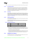
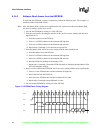
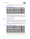
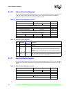
Table 26. MDI Control Register Bits
Bits Field Description
31:30 Reserved Reserved. This field is reserved and returns 0.
29 IE
Interrupt Enable. When this bit is set to 1 by software, it causes the device to assert
an interrupt indicating the end of an MDI cycle.
28 R
Ready. set to 1 by the device at the end of MDI transaction (i.e., indicates a Read or
Write has been completed. It should be reset to 0 by software at the same time the
command is written.
27:26 Opcode
Opcode. For an MDI write, the opcode equals 01b, and for MDI read, 10b. 00b and
11b are reserved and should not be used.
25:21 PHYAdd PHY Address.
20:16 RegAdd
PHY Register Address.
NOTE: This value equals 1 for Intel PRO/100B TX and T4 adapters.
15:0 Data
Data. In a write command, software places the data bits here and the device shifts
them out to the PHY. In a read command the device reads these bits serially from the
PHY and software can read them from this location.