


Intel 8255x 10/100 Mbps Ethernet Controller Family Open Source Software Developer Manual iii
Contents
Contents
1 Introduction....................................................................................................................................1
1.1 Scope....................................................................................................................................1
1.2 Document Conventions ........................................................................................................2
1.2.1 Device References ..................................................................................................2
1.2.2 Numbering ...............................................................................................................2
1.2.3 Signal Name Representation...................................................................................2
1.2.4 Memory Alignment Terminology ..............................................................................2
2 Adapter and Controller Overview ................................................................................................5
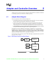
2.1 Adapter Block Diagram.........................................................................................................5
2.2 Intel Fast Ethernet MAC Features ........................................................................................6
2.2.1 82557 Features........................................................................................................6
2.2.2 82558 Features........................................................................................................6
2.2.3 82559, 82550, 82551, and 82562 Features.............................................................7
2.3 Working with the Physical Layer...........................................................................................7
3 Power Management Interface.......................................................................................................9
3.1 Low Power Mode Requirements...........................................................................................9
3.2 Device Power States ............................................................................................................9
3.3 Power Management Registers .............................................................................................9
3.4 Link Operation ....................................................................................................................10
4 PCI Interface.................................................................................................................................11
4.1 PCI Configuration Space ....................................................................................................11
4.1.1 Vendor ID (Offset 0)...............................................................................................12
4.1.2 Device ID (Offset 2) ...............................................................................................12
4.1.3 Command Register (Offset 4)................................................................................12
4.1.4 Status Register (Offset 6) ......................................................................................12
4.1.5 Revision (Offset 8) .................................................................................................13
4.1.6 Class Code (Offset 9) ............................................................................................14
4.1.7 Cache Line Size (Offset C) ....................................................................................14
4.1.8 Latency Timer (Offset D) .......................................................................................14
4.1.9 Header Type (Offset E)..........................................................................................14
4.1.10 Built in Self Test (Offset F).....................................................................................15
4.1.11 Subsystem ID (Offset 2C)......................................................................................16
4.1.12 Subsystem Vendor ID (Offset 2E) .........................................................................16
4.1.13 Expansion ROM Base Address Register (Offset 30).............................................16
4.1.14 The Capabilities Pointer (Offset 34).......................................................................17
4.1.15 Interrupt Line (Offset 3C) .......................................................................................17
4.1.16 Interrupt Pin (Offset 3D).........................................................................................17
4.1.17 Max_Lat / Min_Gnt (Offset 3E) ..............................................................................18
4.1.18 Power Management PCI Configuration Registers .................................................18
4.2 PCI Command Usage.........................................................................................................21
4.2.1 Memory Write and Invalidate .................................................................................22
4.2.2 Read Align .............................................................................................................23
4.2.3 Odd Byte Alignment Support .................................................................................23