


18 Intel 8255x 10/100 Mbps Ethernet Controller Family Open Source Software Developer Manual
PCI Interface
4.1.17 Max_Lat / Min_Gnt (Offset 3E)
These registers specify the device settings for Latency Timer values. For both registers, the value
specifies a period of time in units of ¼ microsecond. Min_Gnt is used to specify the burst length
period the device needs assuming a clock rate of 33 MHz. Max_Lat is used to specify how often
the device needs to gain access to the PCI bus. The values of these registers are 8h (2 µS) for
Min_Gnt and 18h (6 µS) for Max_Lat.
4.1.18 Power Management PCI Configuration Registers
4.1.18.1 Capability Identifier (Offset DC)
The Capability Identifier signals this item in the capability linked list as the PCI Power
Management registers. The PCI Power Management registers have been assigned the ID of 01h.
Since power management is not implemented in the 82557, this register is hard-coded to 0 for that
device. For the 82558 and later devices, this read only register returns 01h.
4.1.18.2 Next Item Pointer (Offset DD)
The Next Item Pointer register describes the location of the next item in the capability list. Since
power management is the last item in the list, this register is set to 0.
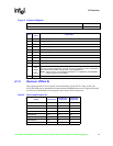
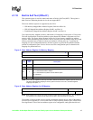
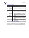
4.1.18.3 Power Management Capabilities (Offset DE)
The Power Management Capabilities (PMC) register is a 16-bit read-only register, which provides
information on the capabilities of the device related to power management. Since power
management is not implemented in the 82557, this register is hard-coded to 0 for that device. For
the 82558 and later devices, this register returns values according to the chart below.
Table 4. Power Management Capabilities
Bit Default Value R / W Description
31:27
82558A: 00011
82558B, 82559:
no auxiliary power
- 01111
with auxiliary
power - 11111
RO
PME_Support. This five bit field indicates the power states in
which the device may assert PME#. A value of 0b for any bit
indicates that the function is not capable of asserting the PME#
signal while in that power state.
The 82558 A-step supports wake-up from D0 and D1. The 82558
B-step and 82559 support wake-up from D0, D1, D2 and D3
hot
if no
auxiliary power is present and from all power states if auxiliary
power exists.
26 1 RO
D2_Support. If this bit is set, this function supports the D2 Power
Management State. All devices must support the D0 and D3 states.
The 82559 and later devices support the D2 Power Management
State.
25 1 RO
D1_Support. If this bit is set, this function supports the D1 Power
Management State. The 82558 and later devices supports the D1
Power Management State.
24
82558A: 1
82558B: 0
82559: 0
RO
FullClk. If this bit is set, this function requires a full speed clock at
all times when it is in the D0 state in order to perform its function. If
this bit is cleared, the function only requires a full speed PCI clock
while actually transferring data so dynamic clock control may be
used. The 82558 A-step requires a full speed clock at all times
when it is in the D0 state in order to perform its function.