


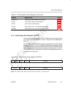

Video Display Registers
4-57Video Display PortSPRU629
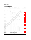
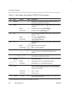
Table 4–7. Video Display Control Register (VDCTL) Field Descriptions (Continued)
Bit
Description
Valuesymval
†
field
†
Bit
Raw Data ModeBT.656 and Y/C Mode
Valuesymval
†
field
†
21 HXS Horizontal external synchronization enable bit.
OUTPUT 0 VCTL1 is an output.
HSINPUT 1 VCTL1 is an external horizontal sync input.
20
VCTL3S VCTL3 output select bit.
CBLNK 0 Output CBLNK
FLD 1 Output FLD
19–18
VCTL2S VCTL2 output select bit.
VYSYNC 0 Output VSYNC
VBLNK 1h Output VBLNK
CSYNC 2h Output CSYNC
FLD 3h Output FLD
17–16
VCTL1S VCTL1 output select bit.
HYSYNC 0 Output HSYNC
HBLNK 1h Output HBLNK
AVID 2h Output AVID
FLD 3h Output FLD
15
VDEN Video display enable bit. Other bits in VDCTL (except RSTCH and
BLKDIS bits) may only be changed when VDEN = 0.
DISABLE 0 Video display is disabled.
ENABLE 1 Video display is enabled.
14
DPK 10-bit packing format select bit.
N10UNPK 0 Normal 10-bit unpacking
D10UNPK 1 Dense 10-bit unpacking
†
For CSL implementation, use the notation VP_VDCTL_field_symval
‡
For complete encoding of these bits, see Table 4–4.