


GPIO Registers
General Purpose I/O Operation5-10 SPRU629
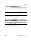
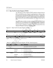
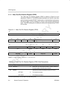
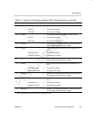
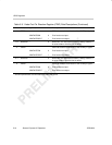
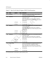
Table 5–5. Video Port Pin Direction Register (PDIR) Field Descriptions (Continued)
Bit DescriptionValuesymval
†
field
†
8 PDIR8 PDIR8 bit controls the direction of the VDATA[9–8] pins.
VDATA8TO9IN 0 Pins function as input.
VDATA8TO9OUT 1 Pins function as output.
7–5
Reserved – 0 Reserved. The reserved bit location is always read as 0.
A value written to this field has no effect.
4 PDIR4 PDIR4 bit controls the direction of the VDATA[7–4] pins.
VDATA4TO7IN 0 Pins function as input.
VDATA4TO7OUT 1 Pins function as output.
3–1
Reserved – 0 Reserved. The reserved bit location is always read as 0.
A value written to this field has no effect.
0 PDIR0 PDIR0 bit controls the direction of the VDATA[3–0] pins.
VDATA0TO3IN 0 Pins function as input.
VDATA0TO3OUT 1 Pins function as output.
†
For CSL implementation, use the notation VP_PDIR_field_symval