


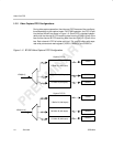
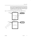
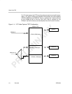
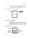
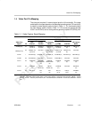
Video Port Pin Mapping
Overview1-14 SPRU629
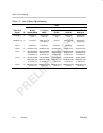
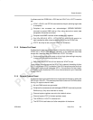
Table 1–2. Video Display Signal Mapping
Usage
Raw Data Display Mode
Video Port
Signal
I/O
BT.656
Display Mode
Y/C Display
Mode
8/10-Bit
16/20-Bit
8/10-Bit
Dual Sync
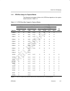
VDATA[9–0] I/O VDOUT[9–0]
(Out)
VDOUT[9–0]
(Out) (Y)
VDOUT[9–0]
(Out)
VDOUT[9–0]
(Out)
VDOUT[9–0]
(Out) (Ch A)
VDATA[19–10] I/O Not Used VDOUT[19–10]
(Out) (Cb/Cr)
Not Used VDOUT[19–10]
(Out)
VDOUT[9–0]
(Out) (Ch B)
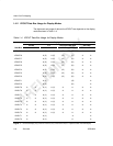
VCLK1 I VCLKIN (In) VCLKIN (In) VCLKIN (In) VCLKIN (In) VCLKIN (In)
VCLK2 I/O VCLKOUT (Out) VCLKOUT (Out) VCLKOUT (Out) VCLKOUT (Out) VCLKOUT (Out)
VCTL1 I/O HSYNC/HBLNK/
AVID/FLD (Out)
or HSYNC (In)
HSYNC/HBLNK/
AVID/FLD (Out)
or HSYNC (In)
HSYNC/HBLNK/
AVID/FLD (Out)
or HSYNC (In)
HSYNC/HBLNK/
AVID/FLD (Out)
or HSYNC (In)
HSYNC/HBLNK/
AVID/FLD (Out)
or HSYNC (In)
VCTL2 I/O VSYNC/VBLNK/
CSYNC/FLD (Out)
or VSYNC (In)
VSYNC/VBLNK/
CSYNC/FLD (Out)
or VSYNC (In)
VSYNC/VBLNK/
CSYNC/FLD (Out)
or VSYNC (In)
VSYNC/VBLNK/
CSYNC/FLD (Out)
or VSYNC (In)
VSYNC/VBLNK/
CSYNC/FLD (Out)
or VSYNC (In)
VCTL3
I/O CBLNK/FLD (Out)
or FLD (In)
CBLNK/FLD (Out)
or FLD (In)
CBLNK/FLD (Out)
or FLD (In)
CBLNK/FLD (Out)
or FLD (In)
CBLNK/FLD (Out)
or FLD (In)