


GPIO Registers
General Purpose I/O Operation5-6 SPRU629
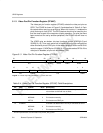
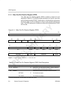
5.1.3 Video Port Pin Function Register (PFUNC)
The video port pin function register (PFUNC) selects the video port pins as
GPIO. The PFUNC is shown in Figure 5–3 and described in Table 5–4. Each
bit controls either one pin or a set of pins. When a bit is set to 1, it enables the
pin(s) that map to it as GPIO. The GPIO feature should not be used for pins
that are used as part of the capture or display operation. For pins that have
been muxed out for use by another peripheral, the PFUNC bits will have no
effect.
The VDATA pins are broken into two functional groups: VDATA[9–0] and
VDATA[19–10]. Thus, each entire half of the data bus must be configured as
either functional pins or GPIO pins. In the case of single BT.656 or raw 8/10-bit
mode, the upper 10 VDATA pins (VDATA[19–10]) can be used as GPIOs. If the
video port is disabled, all pins can be used as GPIO.
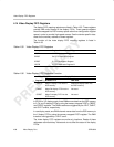
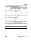
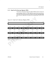
Figure 5–3. Video Port Pin Function Register (PFUNC)
31 23 22 21 20 19 16
Reserved
PFUNC22 PFUNC21 PFUNC20 Reserved
R-0 R/W-0 R/W-0 R/W-0 R/W-0
15 11 10 9 1 0
Reserved
PFUNC10 Reserved PFUNC0
R-0 R/W-0 R-0 R/W-0
Legend: R = Read only; R/W = Read/Write; -n = value after reset
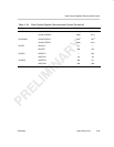
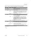
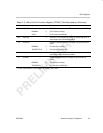
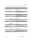
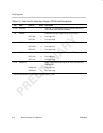
Table 5–4. Video Port Pin Function Register (PFUNC) Field Descriptions
Bit field
†
symval
†
Value Description
31–23 Reserved – 0 Reserved. The reserved bit location is always read as 0. A
value written to this field has no effect.
22 PFUNC22 PFUNC22 bit determines if VCTL3 pin functions as GPIO.
NORMAL 0 Pin functions normally.
VCTL3 1 Pin functions as GPIO pin.
21
PFUNC21 PFUNC21 bit determines if VCTL2 pin functions as GPIO.
NORMAL 0 Pin functions normally.
VCTL2 1 Pin functions as GPIO pin.
†
For CSL implementation, use the notation VP_PFUNC_field_symval