


Video Display Registers
4-65Video Display PortSPRU629
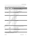
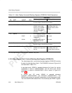
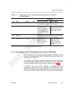
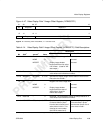
Table 4–11. Video Display Field 1 Vertical Blanking End Register (VDVBLKE1)
Field Descriptions
Description
Bit field
†
symval
†
Value
BT.656 and Y/C Mode
Raw Data Mode
31–28 Reserved – 0 Reserved. The reserved bit location is always read as
0. A value written to this field has no effect.
27–16 VBLNKYSTOP1 OF(value) 0–FFFh Specifies the line (in
FLCOUNT) where
VBLNK inactive edge
occurs for field 1. Does
not affect EAV/SAV V bit
operation.
Specifies the line (in
FLCOUNT) where vertical
blanking ends (VBLNK
inactive edge) for field 1.
15–12 Reserved – 0 Reserved. The reserved bit location is always read as
0. A value written to this field has no effect.
11–0 VBLNKXSTOP1 OF(value) 0–FFFh Specifies the pixel (in
FPCOUNT) where
VBLNK inactive edge
occurs for field 1.
Specifies the pixel (in
FPCOUNT) where
vertical blanking ends
(VBLNK inactive edge)
for field 1.
†
For CSL implementation, use the notation VP_VDVBLKE1_field_symval
4.12.7 Video Display Field 2 Vertical Blanking Start Register (VDVBLKS2)
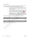
The video display field 2 vertical blanking start register (VDVBLKS2) controls
the start of vertical blanking in field 2. The VDVBLKS2 is shown in Figure 4–45
and described in Table 4–12.
In raw data mode, VBLNK is asserted whenever the frame line counter
(FLCOUNT) is equal to VBLNKYSTART2 and the frame pixel counter (FPCOUNT)
is equal to VBLNKXSTART2 (this is shown in Figure 4–6, page 4-7).
In BT.656 and Y/C mode, VBLNK is asserted whenever
FLCOUNT = VBLNKYSTART2 and FPCOUNT = VBLNKXSTART2. This
VBLNK output control is completely independent of the timing control codes.
The V bit in the EAV/SAV codes for field 2 is controlled by the VDVBIT2 register.