


www.ti.com
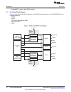
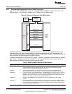
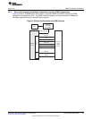
EMAC Functional Architecture
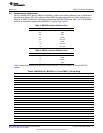
Table 7. EMAC and MDIO Signals for MII Interface
Signal Name I/O Description
MTCLK I Transmit clock (MTCLK). The transmit clock is a continuous clock that provides the timing reference
for transmit operations. The MTXD and MTXEN signals are tied to this clock. The clock is generated
by the PHY and is 2.5 MHz at 10-Mbps operation and 25 MHz at 100-Mbps operation.
MTXD[3:0] O Transmit data (MTXD). The transmit data pins are a collection of 4 data signals comprising 4 bits of
data. MTDX0 is the least-significant bit (LSB). The signals are synchronized by MTCLK and valid
only when MTXEN is asserted.
MTXEN O Transmit enable (MTXEN). The transmit enable signal indicates that the MTXD pins are generating
nibble data for use by the PHY. It is driven synchronously to MTCLK.
MCOL I Collision detected (MCOL). The MCOL pin is asserted by the PHY when it detects a collision on the
network. It remains asserted while the collision condition persists. This signal is not necessarily
synchronous to MTCLK nor MRCLK. This pin is used in half-duplex operation only.
MCRS I Carrier sense (MCRS). The MCRS pin is asserted by the PHY when the network is not idle in either
transmit or receive. The pin is de-asserted when both transmit and receive are idle. This signal is not
necessarily synchronous to MTCLK or MRCLK. This pin is used in half-duplex operation only.
MRCLK I Receive clock (MRCLK). The receive clock is a continuous clock that provides the timing reference
for receive operations. The MRXD, MRXDV, and MRXER signals are tied to this clock. The clock is
generated by the PHY and is 2.5 MHz at 10-Mbps operation and 25 MHz at 100-Mbps operation.
MRXD[3:0] I Receive data (MRXD). The receive data pins are a collection of 4 data signals comprising 4 bits of
data. MRDX0 is the least-significant bit (LSB). The signals are synchronized by MRCLK and valid
only when MRXDV is asserted.
MRXDV I Receive data valid (MRXDV). The receive data valid signal indicates that the MRXD pins are
generating nibble data for use by the EMAC. It is driven synchronously to MRCLK.
MRXER I Receive error (MRXER). The receive error signal is asserted for one or more MRCLK periods to
indicate that an error was detected in the received frame. This is meaningful only during data
reception when MRXDV is active.
MDCLK O Management data clock (MDCLK). The MDIO data clock is sourced by the MDIO module on the
system. It is used to synchronize MDIO data access operations done on the MDIO pin. The
frequency of this clock is controlled by the CLKDIV bits in the MDIO control register (CONTROL).
MDIO I/O Management data input output (MDIO). The MDIO pin drives PHY management data into and out of
the PHY by way of an access frame consisting of start of frame, read/write indication, PHY address,
register address, and data bit cycles. The MDIO pin acts as an output for everything except the data
bit cycles, when the pin acts as an input for read operations.
When the device is interfaced to an Ethernet switch via an MII interface, the carrier sense (MCRS) and
collision (MCOL) signals are not necessary since full-duplex operation is forced.
On the TCI6486/C6472 device, the MII Ethernet interface is available only on EMAC0. MII0 pins are
multiplexed with other non-RGMII pins (RMII1, S3MII1). due to this multiplexing, when the MII0 interface is
selected on EMAC0, except for RGMII1, no Ethernet interface is available on EMAC1.
19
SPRUEF8F–March 2006–Revised November 2010 C6472/TCI6486 EMAC/MDIO
Submit Documentation Feedback
Copyright © 2006–2010, Texas Instruments Incorporated