


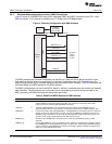
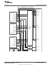

RGTXC
RGTXD[3−0]
RGTXCTL
RGREFCLK
RGRXC
RGRXD[3−0]
RGRXCTL
RGMDCLK
RGMDIO
Physical
layer
device
(PHY)
System
core
Transformer
2.5 MHz
25 MHz,
or 125 MHz
RJ−45
EMAC
MDIO
www.ti.com
EMAC Functional Architecture
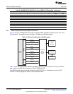
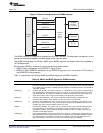
Figure 5. Ethernet Configuration with RGMII Interface
The RGMII interface is a reduced pin alternative to the GMII interface. The data paths are reduced, control
signals are multiplexed together, and both edges of the clock are used.
The RGMII interface does not include a MCOL and a MCRS signal for half-duplex mode (only available in
10/100 Mbps mode).
Carrier sense (MCRS) is indicated by one of the following cases instead:
• MRXDV signal (multiplexed in the RGRXCTL signal) is true
• MRXDV is false, MRXERR (multiplexed in the RGRXCTL signal) is true, and a value of FFh exists on
the RGRXD[3:0] simultaneously
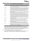
Table 10 summarizes the individual EMAC and MDIO signals for the RGMII interface.
Table 10. EMAC and MDIO Signals for RGMII Interface
Signal Name I/O Description
RGTXC O Transmit clock (RGTXC). The transmit clock is a continuous clock that provides the timing reference
for transmit operations. The RGTXD and RGTXCTL signals are tied to this clock. The clock is driven
by the EMAC and is 2.5 MHz at 10-Mbps operation, 25 MHz at 100-Mbps operation, and 125 MHz at
1000-Mbps operation.
RGTXD[3-0] O Transmit data (RGTXD). The transmit data pins are a collection of 4 data signals comprising 4 bits of
data. RGTDX0 is the least-significant bit (LSB). The signals are synchronized by RGTXC and valid
only when RGTXCTL is asserted. The lower 4 bits of data are transmitted on the rising edge of the
clock, and the higher 4 bits of data are transmitted on the falling edge of the RGTXC.
RGTXCTL O Transmit enable (RGTXCTL). The transmit enable signal indicates that the RGTXD pins are
generating nibble data for use by the PHY. It is driven synchronously to RGTXC.
RGREFCLK O Reference clock (RGREFCLK). This 125-MHz reference clock is provided as a convenience. It can
be used as a clock source to the PHY, so that the PHY may generate the RGRXC clock to be sent
to EMAC. This clock is stopped while the device is in reset.
RGRXC I Receive clock (RGRXC). The receive clock is a continuous clock that provides the timing reference
for receive operations. The RGRXD, and RGRXCTL signals are tied to this clock. The clock is
generated by the PHY and is 2.5 MHz at 10-Mbps operation, 25 MHz at 100-Mbps operation, and
125 MHz at 1000-Mbps operation.
RGRXD[3-0] I Receive data (RGRXD). The receive data pins are a collection of 4 data signals comprising 4 bits of
data. RGRDX0 is the least-significant bit (LSB). The signals are synchronized by RGRXC and valid
only when RGRXCTL is asserted. The lower 4 bits of data are received on the rising edge of the
clock, and the higher 4 bits of data are received on the falling edge of the RGRXC.
23
SPRUEF8F–March 2006–Revised November 2010 C6472/TCI6486 EMAC/MDIO
Submit Documentation Feedback
Copyright © 2006–2010, Texas Instruments Incorporated