


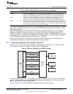
MDCLK
MDIO
RMTXD[1−0]
RMTXEN
RMCRSDV
RMRXD[1−0]
RMRXER
Physical
layer
device
(PHY)
EMAC
MDIO
System
core
RMREFCLK RMREFCLK
50-MHz
zero-delay
clock buffer
50-MHz
XO
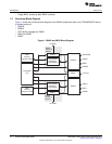
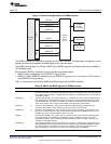
EMAC Functional Architecture
www.ti.com
2.3.2 Reduced Media Independent Interface (RMII) Connections
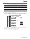
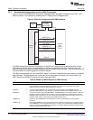
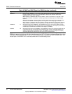
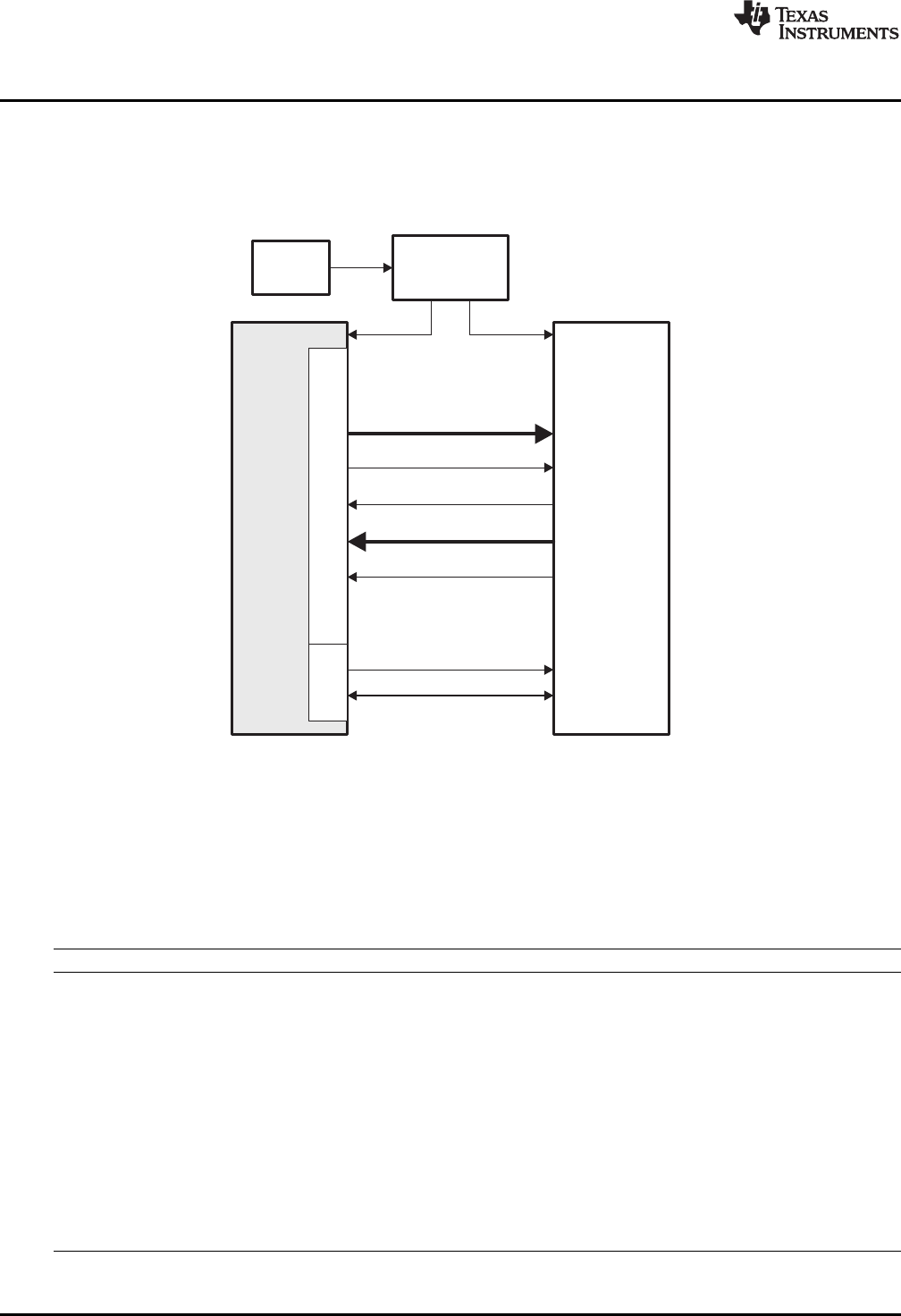
Figure 3 shows a TCI6486/C6472 device with integrated EMAC and MDIO interfaced to the PHY via an
RMII connection. This interface is available only in 10-Mbps and 100-Mbps modes.
Figure 3. Ethernet Configuration with RMII Interface
The RMII interface has the same functionality as the MII, but it does so with a reduced number of pins,
thus lowering the total cost for an application. In devices incorporating many PHY interfaces such as
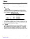
switches, the number of pins can add significant cost as the port counts increase. Table 8 summarizes the
individual EMAC and MDIO signals for the RMII interface.
The RMII interface does not include an MCOL signal. A collision is detected from the receive and transmit
data delimiters. The data signals are 2 bits wide, and a single reference clock must be provided to the
MAC, operating at 50 MHz to sustain the same data rate as MII.
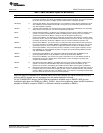
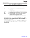
Table 8. EMAC and MDIO Signals for RMII Interface
Signal Name I/O Description
RMTXD[1-0] O Transmit data (RMTXD). The transmit data pins are a collection of 2 data signals comprising 2 bits
of data. RMTDX0 is the least-significant bit (LSB). The signals are synchronized to the RMII
reference clock and valid only when RMTXEN is asserted.
RMTXEN O Transmit enable (RMTXEN). The transmit enable signal indicates that the RMTXD pins are
generating nibble data for use by the PHY. It is driven synchronously to the RMII reference clock.
RMCRSDV I Carrier sense/receive data valid (RMCRSDV). The RMCRSDV pin is asserted by the PHY when the
network is not idle in either transmit or receive. The data on RMRXD is considered valid once the
RMCRSDV signal is asserted. The pin is de-asserted when both transmit and receive are idle. The
assertion of this signal is asynchronous to the RMII reference clock.
RMREFCLK I Reference clock (RMREFCLK). A 50-MHz clock must be provided through this pin for RMII
operation.
RMRXD[1-0] I Receive data (RMRXD). The receive data pins are a collection of 2 data signals comprising 2 bits of
data. RMRDX0 is the least-significant bit (LSB). The signals are synchronized to the RMII reference
clock and valid only when RMCRSDV is asserted. In 10-Mbps operation, RMRXD is sampled every
tenth cycle of the RMII reference clock.
20
C6472/TCI6486 EMAC/MDIO SPRUEF8F–March 2006–Revised November 2010
Submit Documentation Feedback
Copyright © 2006–2010, Texas Instruments Incorporated