


MuxOneNAND2G(KFM2G16Q2A-DEBx)
- 102 -
FLASH MEMORY
MuxOneNAND4G(KFN4G16Q2A-DEBx)
3.9.3 4-, 8-, 16-, 32-, 1K- Word Linear Burst Read Operation During Synchronous Burst Block Read Mode
Same as normal linear burst read, synchronous burst block read enables a fixed number of words to be read from consecutive address.
The device supports a burst read from consecutive addresses of 4-, 8-, 16-, 32- and 1K-words with no wrap.
(note that wrap-around is not supported in Synchronous Burst Block Read)
3.9.4 Programmable Burst Read Latency Operation During Synchronous Burst Block Read Mode
Synchronous burst block read mode have programmable burst read latency just same manner as normal synchronous burst read mode.
Upon power up, the number of initial clock cycles from Valid Address (AVD
) to initial data defaults to four clocks.
The number of clock cycles (n) which are inserted after the clock which is latching the address. The host can read the first data with the
(n+1)th rising edge.
The number of total initial access cycles is programmable from three to seven cycles. After the number of programmed burst clock cycles is
reached, the rising edge of the next clock cycle triggers the next burst data.
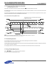
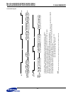
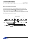
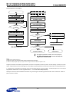
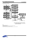
Four Clock Burst Read Latency (default condition)
tIAA
Hi-Z
CE
CLK
AVD
OE
RDY
tRDYA
A/DQ0:
A/DQ15
D6 D7 D0 D1 D2 D3 D7 D0
Hi-Z
Valid
Address
-10123
tBA
Rising edge of the clock cycle following last read latency
triggers next burst data
tRDYS
4