


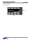

MuxOneNAND2G(KFM2G16Q2A-DEBx)
- 109 -
FLASH MEMORY
MuxOneNAND4G(KFN4G16Q2A-DEBx)
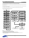
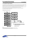
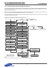
3.11.2 2X Cache Program Operation
See Timing Diagram 6.14
The 2X Cache Program Operation is invented to accomplish continuous 2X Program Operation efficiently by hiding transferring time from Dat-
aRAM to page buffer..
1. 4KB Data write from host to DataRAMs.
2. 2X Cache Program command issue. This will turn INT pin to busy state
1)
, OnGo bit sets to ‘1’.
(Note that before issuing ‘2X Cache Program Command’, host should make sure that the target blocks are unlocked.)
3. 4KB data will be trasfered to each page buffer in two-plane NAND Flash Array at the same time.
4. When this transfer operation is complete, programming into NAND Flash Array will automatically start, and at the same time, INT bit will turn
to ‘1’ to indicate that DataRAMs are now ready to be written with next 4KB data.
5. When second 4KB is written to two DataRAMs, another 2X Cache Program command is issued and INT bit will go to ‘0’
1)
.
NOTE :
1) this is for INT auto mode, for INT manual mode case, user should write 0 to INT bit before issuing any command.
If host wants to program data under 4 sector size, unwanted area to be programmed must be written to all ‘1’s.
(BSC must be set to 00, which is 4sectors.)
When INT bit goes to ‘1’ after second data transfer from DataRAMs to Pafe Buffers are complete, user may check the Status Register to check
the 2X program status. During 2X Cache Program, Error bit shows the status of previous program operation.
For the final 4KB program of 2X Cache Program scheme, host should issue 2X Program Command(007Dh). When the final two pages are
programmed, INT bit will turn to ‘1’ and OnGo status bit - which indicates the overall 2X Cache Program ongoing status - will go to ‘0’. At the
completion of 2X Cache Program operation, Error bit will show the pass/fail status overall status of 2X program, and Plane1 previous[4] ~
Plane2 current[1] bit will show where the error occured accordingly .
Note that 2X Cache Programm command cannot be performed on OTP block and 1st block OTP.
NOTE :
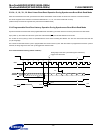
The page number of Page A and Page B is identical in different block.
If Page A is ith page of block 2j, Page B must be ith page of block 2j+1. (j=0,1,2,3...)
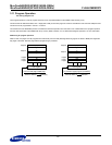
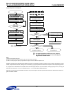
Page A
2) Program
2) Program
DataRAM1
1) Data Write
1) Data Write
3) Data Write
(During step 2 when INT bit goes to ‘1’)
3) Data Write
(during step 2 when INT bit goes to ‘1’)
DataRAM0
Page B
Plane1
Plane2