


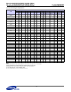
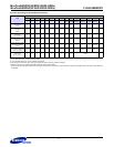

MuxOneNAND2G(KFM2G16Q2A-DEBx)
- 77 -
FLASH MEMORY
MuxOneNAND4G(KFN4G16Q2A-DEBx)
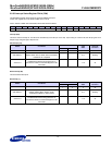
2.8.23 Start Block Address Register F24Ch (R/W)
This Read/Write register shows the NAND Flash block address in the Write Protection mode. Setting this register precedes a 'Lock Block'
command, 'Unlock Block' command, or ‘Lock-Tight' Command.
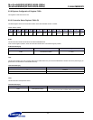
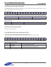
F24Ch, default = 0000h
SBA Information[10:0]
2.8.24 End Block Address Register F24Dh
This register is reserved for future use.
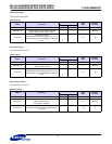
2.8.25 NAND Flash Write Protection Status Register F24Eh (R)
This Read register shows the Write Protection Status of the NAND Flash memory array.
To read the write protection status, FBA(DFS and DBS also in case of DDP) has to be set before reading the register
.
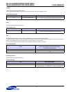
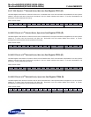
F24Eh, default = 0002h
Write Protection Status Information[2:0]
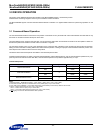
15 14 13 12 11 10 9 8 7 6 5 4 3 2 1 0
Reserved(000000) SBA
Device Number of Block SBA
2Gb 2048 [10:0]
Item Definition Description
SBA Start Block Address Precedes Lock Block, Unlock Block, or Lock-Tight commands
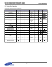
15 14 13 12 11 10 9 8 7 6 5 4 3 2 1 0
Reserved(0000000000000) US LS LTS
Item Definition Description
US Unlocked Status 1 = current NAND Flash block is unlocked
LS Locked Status
1 = current NAND Flash block is locked
Or First Block of NAND Flash Array is Locked to be OTP
LTS Locked-Tight Status 1 = current NAND Flash block is locked-tight