


MuxOneNAND2G(KFM2G16Q2A-DEBx)
- 141 -
FLASH MEMORY
MuxOneNAND4G(KFN4G16Q2A-DEBx)
5.0 AC CHARACTERISTICS
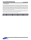
5.1 AC Test Conditions
5.2 Device Capacitance
CAPACITANCE(TA = 25 C, VCC = 1.8V, f = 1.0MHz)
NOTE :
Capacitance is periodically sampled and not 100% tested.
5.3 Valid Block Characteristics
NOTE :
1) The
device may include invalid blocks when first shipped. Additional invalid blocks may develop while being used. The number of valid blocks is presented with
both cases of invalid blocks considered. Invalid blocks are defined as blocks that contain one or more bad bits
. Do not erase or program factory-marked bad
blocks.
2) The 1st block, which is placed on 00h block address, is guaranteed to be a valid block up to 1K program/erase cycles with 1bit/512Byte ECC.
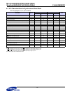
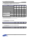
Parameter Value (66MHz) Value (83MHz)
Input Pulse Levels 0V to V
CC 0V to VCC
Input Rise and Fall Times
CLK 3ns 2ns
other inputs 5ns 2ns
Input and Output Timing Levels
VCC/2 VCC/2
Output Load
C
L = 30pF CL = 30pF
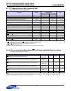
Item Symbol Test Condition
Single DDP Unit
Min Max Min Max
Input Capacitance CIN1 VIN=0V - 10 - 20 pF
Control Pin Capacitance C
IN2
VIN=0V
- 10 - 20 pF
Output Capacitance C
OUT VOUT=0V - 10 - 20 pF
INT Capacitance C
INT VOUT=0V - 10 - 20 pF
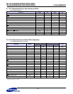
Parameter Symbol Min Typ. Max Unit
Valid Block Number
Single
N
VB
2008 - 2048 Blocks
DDP 4016 - 4096 Blocks
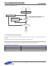
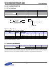
Output Load
Device
Under
Tes t
* CL = 30pF including scope
and Jig capacitance
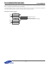
0V
V
CC
VCC/2
V
CC/2
Input Pulse and Test Point
Input & Output
Test Point