


MuxOneNAND2G(KFM2G16Q2A-DEBx)
- 62 -
FLASH MEMORY
MuxOneNAND4G(KFN4G16Q2A-DEBx)
2.8.17 Start Buffer Register F200h (R/W)
This Read/Write register describes the BufferRAM Sector Count (BSC) and BufferRAM Sector Address (BSA).
The BufferRAM Sector Count (BSC) field specifies the number of sectors to be loaded, programmed, or copy back programmed. At 00 value
(the default value), the number of sector is "4". If the internal RAM buffer reaches its maximum value of 11, it will count up to 0 value to meet
the BSC value. For example, if BSA = 1101, BSC = 00, then the selected BufferRAM will count up from '1101
1110 1111 1100'.
The BufferRAM Sector Address (BSA) is the sector 0~3 address in the internal BootRAM and DataRAM where data is placed.
F200h, default = 0000h
NOTE :
In case of ’Cache Read’, BSA has to be set to 1000 or 1100. And BSC has to be set to 00.
In case of ’Synchronous Burst Block Read’, BSA has to be set to 1000 . And BSC has to be set to 00.
In case of ’2X Program’ or ’2X Cache Program’, BSA has to be set to 1000. And BSC has to be set to 00.
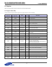
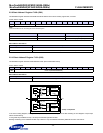
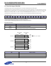
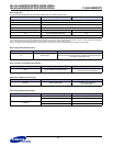
Start Address8 Information
15 14 13 12 11 10 9 8 7 6 5 4 3 2 1 0
Reserved(0000) BSA Reserved(000000) BSC
Item Description
BSA[3] Selection bit between BootRAM and DataRAM
BSA[2] Selection bit between DataRAM0 and DataRAM1
BSA[1:0]
Selection bit between Sector0 and Sector1 in the internal BootRAM
Selection bit between Sector0 to Sector3 in the internal DataRAM
BSC Number of Sectors
01 1 sector
10 2 sector
11 3 sector
00 4 sector
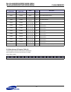
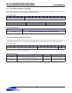
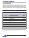
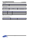
BootRAM 0
BootRAM 1
BootRAM
Sector: (512 + 16) Byte
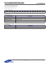
DataRAM 1_0
DataRAM 1_1
DataRAM 1_2
DataRAM 1_3
DataRAM1
0000
0001
1100
1101
1110
1111
Main area data
Spare area data
BSA
DataRAM 0_0
DataRAM 0_1
DataRAM 0_2
DataRAM 0_3
DataRAM0
1000
1001
1010
1011
512B
16B