


MuxOneNAND2G(KFM2G16Q2A-DEBx)
- 145 -
FLASH MEMORY
MuxOneNAND4G(KFN4G16Q2A-DEBx)
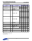
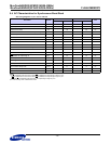
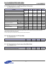
5.9 AC Characteristics for Load/Program/Erase Performance
See Timing Diagrams 6.11, 6.12, and 6.16
NOTE :
1) These parameters are tested based on INT bit of interrupt register. Because the time on INT pin is related to the pull-up and pull-down resistor value.
2) Spare Load time is little bit less than Sector Load time.
3) Spare Program time is same as Sector program time.
4) 2/3 sector Load/Program time is between Sector Load/Progrma time and Page Load/Program time.
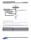
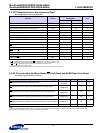
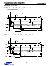
5.10 AC Characteristics for INT Auto Mode
See Timing Diagrams 6.25
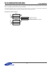
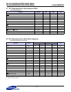
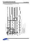
5.11 AC Characteristics for Synchronous Burst Block Read
See Timing Diagrams 6.3, 6.4
Parameter Symbol Min Typ Max Unit
Spare Load time(Note 1, Note2)
tRD1 - 23 35 s
Sector Load time(Note 1)
Page Load time(Note 1) tRD2 - 30 45 s
Spare Program time(Note 1, Note3)
tPGM1 - 205 720 s
Sector Program time(Note 1)
Page Pogram time(Note 1) tPGM2 - 220 750 s
OTP Access Time(Note 1) tOTP - 500 700 ns
Lock/Unlock/Lock-tight (Note 1) tLOCK - 500 700 ns
All Block Unlock Time tABU - 2 3 s
Erase Suspend Time (Note 1) tESP - 400 500 s
Erase Resume Time(Note 1)
1 Block tERS1 - 1.5 2 ms
2~64 Blocks tERS2 4 6 ms
Number of Partial Program Cycles in the page (Including main
and spare area)
NOP - - 4 cycles
Block Erase time (Note 1)
1 Block tBERS1 - 1.5 2 ms
2~64 Blocks tBERS2 - 4 6 ms
Multi Block Erase Verify Read time(Note 1) tRD3 - 70 100 s
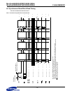
Parameter Symbol
Min Max
Unit
Command Input to INT Low
tWB
- 200 ns
Parameter Symbol
Typ. Max
Unit
INT Low Period During Synch Burst Block Read
tINTL
1-us