


MuxOneNAND2G(KFM2G16Q2A-DEBx)
- 61 -
FLASH MEMORY
MuxOneNAND4G(KFN4G16Q2A-DEBx)
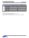
2.8.13 Start Address5 Register F104h (R/W)
This Read/Write register describes the number of page in Synchronous Burst Block Read.
F104h, default = 0000h
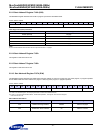
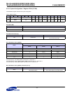
Flash Page Count (FPC) Information
NOTE :
Synchronous Burst Block Read are NOT able to be perforformed with 1 or 2pages.
2.8.14 Start Address6 Register F105h
This register is reserved for future use.
2.8.15 Start Address7 Register F106h
This register is reserved for future use.
2.8.16 Start Address8 Register F107h (R/W)
This Read/Write register describes the NAND Flash start page address in a block for a page load, copy back program, or program operation
and the NAND Flash start sector address in a page for a load, copy back program, or program operation.
F107h, default = 0000h
NOTE :
1) In case of ‘2X Cache Program’, the host programs data on same FPA of different Planes.
2) In case of ‘ Synchronous Burst Block Read’, ‘Cache Read Operation’, ‘2X Program’ and ‘2X Cache Program’,
FSA has to be set to 00.
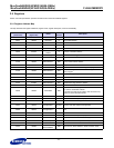
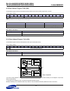
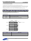
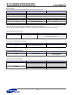
Start Address8 Information
15 14 13 12 11 10 9 8 7 6 5 4 3 2 1 0
Reserved(0000000000) FPC
FPC Number of Page
000000 (Default) 64 page
000011 3 page
000100 4 page
.. ..
111111 63 page
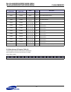
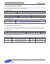
15 14 13 12 11 10 9 8 7 6 5 4 3 2 1 0
Reserved (00000000)
FPA
1)
FSA
2)
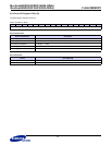
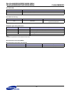
Item Description Default Value Range
FPA NAND Flash Page Address 000000
000000 ~ 111111,
6 bits for 64 pages
FSA NAND Flash Sector Address 00
00 ~ 11,
2 bits for 4 sectors