


MuxOneNAND2G(KFM2G16Q2A-DEBx)
- 12 -
FLASH MEMORY
MuxOneNAND4G(KFN4G16Q2A-DEBx)
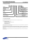
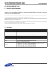
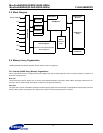
2.5 Block Diagram
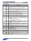
2.6 Memory Array Organization
The MuxOneNAND architecture integrates several memory areas on a single chip.
2.6.1 Internal (NAND Array) Memory Organization
The on-chip internal memory is a single-level-cell (SLC) NAND array used for data storage and code. The internal memory is divided into a
main area and a spare area.
Main Area
The main area is the primary memory array. This main area is divided into Blocks of 64 Pages. Within a Block, each Page is 2KB and is com-
prised of 4 Sectors. Within a Page, each Sector is 512B and is comprised of 256 Words.
Spare Area
The spare area is used for invalid block information and ECC storage. Spare area internal memory is associated with corresponding main area
memory. Within a Block, each Page has four 16B Sectors of spare area. Each spare area Sector is 8 words.
BootRAM
Host Interface
CLK
CE
OE
WE
RP
AVD
StateMachine
Bootloader
Internal Registers
(Address/Command/Configuration
/Status Registers)
Error
Correction
Logic
INT
DataRAM0
BufferRAM
NAND Flash
Array
OTP
(One Block)
RDY
ADQ15~ADQ0
DataRAM1
1st Block OTP
(Block 0)